SBOS456H September 2008 – February 2015 REF5020A-Q1 , REF5025A-Q1 , REF5030A-Q1 , REF5040A-Q1 , REF5045A-Q1 , REF5050A-Q1
PRODUCTION DATA.
- 1 Features
- 2 Applications
- 3 Description
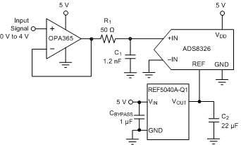
- 4 Simplified Schematic
- 5 Revision History
- 6 Pin Configuration and Functions
- 7 Specifications
- 8 Detailed Description
- 9 Application and Implementation
- 10Power Supply Recommendations
- 11Layout
- 12Device and Documentation Support
- 13Mechanical, Packaging, and Orderable Information
Package Options
Mechanical Data (Package|Pins)
- D|8
Thermal pad, mechanical data (Package|Pins)
Orderable Information
1 Features
- Qualified for Automotive Applications
- Low Temperature Drift
- Standard Grade: 8 ppm/°C (max)
- High Accuracy
- Standard Grade: 0.1% (max)
- Low Noise: 3 μVPP/V
- Excellent Long-Term Stability:
- 5 ppm/1000 hr (typ) after 1000 hours
- High Output Current: ±10 mA
- Temperature Range: –40°C to 125°C
2 Applications
- 16-Bit Data Acquisition Systems
- ATE Equipment
- Industrial Process Control
- Medical Instrumentation
- Optical Control Systems
- Precision Instrumentation
3 Description
The REF50xxA-Q1 family of devices is low-noise, low-drift, very-high precision-voltage reference. These reference devices are capable of both sinking and sourcing, and are very robust with regard to line and load changes.
Excellent temperature drift (3 ppm/°C) and high accuracy (0.05%) are achieved using proprietary design techniques. These features combined with very low noise make the REF50xxA-Q1 family of devices ideal for use in high-precision data acquisition systems.
Each reference voltage is available in a standard-grade versions. The devices are offered in SO-8 packages and are specified from –40°C to 125°C.
Device Information(1)
| PART NUMBER | PACKAGE | OUTPUT VOLTAGE |
|---|---|---|
| REF5020A-Q1 | SOIC (8) | 2.048 V |
| REF5025A-Q1 | 2.5 V | |
| REF5030A-Q1 | 3 V | |
| REF5040A-Q1 | 4.096 V | |
| REF5045A-Q1 | 4.5 V | |
| REF5050A-Q1 | 5 V |
- For all available packages, see the orderable addendum at the end of the data sheet.
4 Simplified Schematic