SNVSCN7B November 2023 – June 2024 REF54
PRODUCTION DATA
- 1
- 1 Features
- 2 Applications
- 3 Description
- 4 Device Comparison Table
- 5 Pin Configuration and Functions
-
6 Specifications
- 6.1 Absolute Maximum Ratings
- 6.2 ESD Ratings
- 6.3 Recommended Operating Conditions
- 6.4 Thermal Information
- 6.5 Electrical Characteristics REF54250
- 6.6 Electrical Characteristics REF54300
- 6.7 Electrical Characteristics REF54410
- 6.8 Electrical Characteristics REF54450
- 6.9 Electrical Characteristics REF54500
- 6.10 Typical Characteristics
- 7 Parameter Measurement Information
- 8 Detailed Description
- 9 Application and Implementation
- 10Device and Documentation Support
- 11Revision History
- 12Mechanical, Packaging, and Orderable Information
Package Options
Mechanical Data (Package|Pins)
- D|8
Thermal pad, mechanical data (Package|Pins)
Orderable Information
7.5 Solder Heat Shift
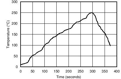
The packaging materials of the REF54 have different coefficients of thermal expansion than the PCB material, resulting in stress change on the device die when the part is heated during soldering process and cooled down afterwards. Thermal shock due to reflow and stress change on the device die causes the output voltages to shift, degrading the initial accuracy performance of the product. Reflow soldering is a common cause of this error. To quantify the impact, 32 devices were soldered on printed circuit boards using lead-free solder paste and the paste manufacturer suggested reflow profile to illustrate this effect. The reflow profile is as shown in Figure 7-12. The printed circuit board is comprised of FR4 material. The board thickness is 1.65 mm and the area is 137 mm × 168 mm.
For recommended reflow profiles using 'Sn-Pb Eutectic Assembly' or 'Pb-Free Assembly' please refer JEDEC J-STD-020 standard.
 Figure 7-12 Reflow Profile
The reference output voltage is measured before and after the reflow process. Solder shift depends on the size, thickness, and material of the printed circuit board. An important note is that the Figure 7-13 displays the typical shift for exposure to a single reflow profile. Exposure to multiple reflows, as is common on PCBs with surface-mount components on both sides, causes additional shifts in the output voltage. If the PCB is exposed to multiple reflows, the device must be soldered in the last pass to minimize the exposure to thermal stress.
 Figure 7-13 Solder Shift