SBOS747B May 2016 – August 2016 REF6125 , REF6130 , REF6133 , REF6141 , REF6145 , REF6150
PRODUCTION DATA.
- 1 Features
- 2 Applications
- 3 Description
- 4 Revision History
- 5 Device Comparison Table
- 6 Pin Configuration and Functions
- 7 Specifications
- 8 Parameter Measurement Information
- 9 Detailed Description
- 10Applications and Implementation
- 11Power Supply Recommendations
- 12Layout
- 13Device and Documentation Support
- 14Mechanical, Packaging, and Orderable Information
Package Options
Mechanical Data (Package|Pins)
- DGK|8
Thermal pad, mechanical data (Package|Pins)
Orderable Information
9.3.1 Integrated ADC Drive Buffer
Many ADC data sheets specify a few microamps of average current draw from the REF pin. Almost all voltage references provide these few microamps of average current; but not all voltage references are practical for driving a high-resolution, high-throughput SAR ADC because the peak current drawn can be very high when the capacitors are switched on the REF pin. The worst-case demand for the voltage reference is during a burst-mode conversion, when the ADC is idle for a very long time, before a conversion is initiated, and the first sample converted is expected to be precise. Usually, a large capacitor is connected between the REF pin and ground pin (or sometimes between the REFP and REFM pins) of the ADC to smoothen the current load and reduce the burden on the voltage reference. The voltage reference must then be capable of providing the average current required to completely charge the reference capacitor, but without causing the reference voltage to droop significantly. Most voltage references lack the ability to completely charge the reference capacitor, and settle when the binary-weighted capacitors are being switched onto the REF pin because of the large output impedance. Usually, voltage references have output impedances in the range of 10's of ohms at frequencies higher than 100 Hz. The output voltage of the voltage reference must be buffered with a low output impedance (usually high bandwidth) amplifier to achieve excellent linearity and distortion performance.
The key amplifier specifications to be considered when designing a reference buffer for a high-precision ADC are: low offset, low drift, wide bandwidth, and low output impedance. While it is possible to select an amplifier that sufficiently meets all these requirements, the amplifier comes at a cost of excessive power consumption. For example, the OPA350 is a 38-MHz bandwidth amplifier with a maximum offset of 0.5 mV, and low offset drift of 4 µV/ºC, but consumes a quiescent current of 5.2mA. This is because (from an amplifier design perspective) offset and drift are dc specifications, whereas bandwidth, low output impedance, and high capacitive drive capability are high-frequency specifications. Therefore, achieving all the performance in one amplifier requires power. However, a more efficient design to meet the low power budget is to use a composite reference buffer, which uses an amplifier with superior high-frequency specifications in the feedback loop of a dc precision amplifier to get the overall performance at much lower power consumption. Figure 49 shows such a composite amplifier design with the OPA333 (dc precision amplifier) and THS4281 (high-bandwidth amplifier). This reference buffer design requires three devices, and a large number of external components. This solution still consumes close to 2 mA of quiescent current.
 Figure 49. Composite Amplifier Reference Buffer
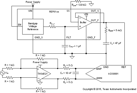
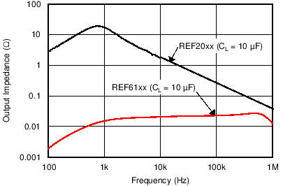
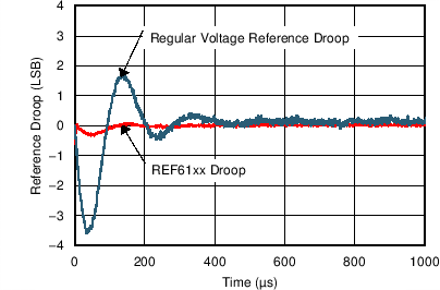
The REF61xx family of voltage references have an integrated low output impedance buffer (ADC drive buffer); therefore, there is no need for an external buffer while driving the REF pin of high-precision, high-throughput SAR ADCs, as shown in Figure 50. The ADC drive buffer of the REF61xx is capable of replenishing a charge of 70 pC on a 47-µF capacitor in 1 µs, without allowing the voltage on the capacitor to droop more than 1 LSB at 18-bit precision. The REF61xx are trimmed at multiple temperatures in production, achieving a max drift of just 8 ppm/°C for both the voltage reference and the buffer combined, while operating at a typical quiescent current of 820 µA. Figure 51 compares the output impedance of a regular voltage reference (REF20xx) and a voltage reference with integrated ADC drive buffer (REF61xx). Figure 52 compares the burst-mode, reference-settling performance of a regular voltage reference and the REF61xx.
 Figure 50. REF61xx Driving REF Pin of ADS8881 SAR ADC

| 1 LSB = 19.07 µV, with ADS8881 at 1 MSPS |