SBOS748 September 2016 REF6225 , REF6230 , REF6233 , REF6241 , REF6245 , REF6250
PRODUCTION DATA.
- 1 Features
- 2 Applications
- 3 Description
- 4 Revision History
- 5 Device Comparison Table
- 6 Pin Configuration and Functions
- 7 Specifications
- 8 Parameter Measurement Information
- 9 Detailed Description
- 10Applications and Implementation
- 11Power Supply Recommendations
- 12Layout
- 13Device and Documentation Support
- 14Mechanical, Packaging, and Orderable Information
Package Options
Mechanical Data (Package|Pins)
- DGK|8
Thermal pad, mechanical data (Package|Pins)
Orderable Information
8.1 Solder Heat Shift
The materials used in the manufacture of the REF62xx have differing coefficients of thermal expansion, and result in stress on the device die when the part is heated. Mechanical and thermal stress on the device die sometimes causes the output voltages to shift, degrading the initial accuracy specifications of the product. Reflow soldering is a common cause of this error.
In order to illustrate this effect, a total of 128 devices were soldered on eight printed circuit boards (PCBs), with 16 devices on each PCB, using lead-free solder paste, and the manufacturer-suggested reflow profile. The reflow profile is as shown in Figure 39. The printed circuit board is comprised of FR4 material. The board thickness is 1.65 mm and the area is 101.6 mm × 127 mm.
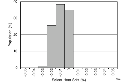
The reference output voltage is measured before and after the reflow process; the typical shift is displayed in Figure 40. Although all tested units exhibit very low shifts (< 0.03%), higher shifts are also possible depending on the size, thickness, and material of the PCB.
The histogram displays the typical shift for exposure to a single reflow profile. Exposure to multiple reflows, as is common on PCBs with surface-mount components on both sides, causes additional shifts in the output bias voltage. If the PCB is exposed to multiple reflows, solder the device in the final pass to minimize exposure to thermal stress.
 Figure 39. Reflow Profile
 Figure 40. Solder Heat Shift Distribution