SBAS221H December 2001 – October 2015 REG71050 , REG71055
PRODUCTION DATA.
- 1 Features
- 2 Applications
- 3 Description
- 4 Revision History
- 5 Device Comparison Table
- 6 Pin Configuration and Functions
- 7 Specifications
- 8 Detailed Description
- 9 Application and Implementation
- 10Power Supply Recommendations
- 11Layout
- 12Device and Documentation Support
- 13Mechanical, Packaging, and Orderable Information
Package Options
Mechanical Data (Package|Pins)
- DDC|6
Thermal pad, mechanical data (Package|Pins)
Orderable Information
8 Detailed Description
8.1 Overview
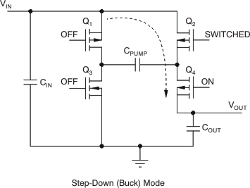
The REG710 regulated charge pump provides a regulated output voltage for input voltages which are not regulated with a value that can be lower or higher than the regulated output voltage. This is accomplished by automatic mode switching within the device. When the input voltage is greater than the required output, the device operates as a variable frequency switched-mode regulator. This operation is shown in Figure 5. Transistors Q1 and Q3 are held off, Q4 is on, and Q2 is switched as needed to maintain a regulated output voltage.
When the input voltage is less than the required output voltage, the device switches to a step-up or boost mode of operation, as shown in Figure 6.
A conversion clock of 50% duty cycle is generated. During the first half cycle the FET switches are configured as shown in Figure 6 (A), and CPUMP charges to VIN.
During the second half cycle the FET switches are configured as shown in Figure 6 (B), and the voltage on CPUMP is added to VIN. The output voltage is regulated by skipping clock cycles as necessary.
 Figure 5. Simplified Schematic of the REG710 Operating in the Step-Down Mode
 Figure 6. Simplified Schematic of the REG710 Operating in the Step-Up or Boost Mode
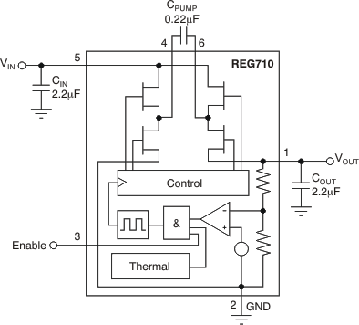
8.2 Functional Block Diagram

8.3 Feature Description
8.3.1 Shutdown Mode
The EN pin enables the IC when pulled high and places it into energy-saving shutdown mode when pulled low. When in shutdown mode, the output is disconnected from the input and the quiescent current is reduced to 0.01 μA typical. This shutdown mode functionality is only valid when VIN is above the minimum recommended operating voltage. The EN pin cannot be left floating and must be actively terminated either high or low.
8.3.2 Protection
The regulator includes thermal shutdown circuitry protecting the device from damage caused by overload conditions. The thermal protection circuitry disables the output when the junction temperature reaches approximately 160°C, allowing the device to cool. When the junction temperature cools to approximately 140°C, the output circuitry is automatically reenabled. Continuously operating the regulator into thermal shutdown can degrade reliability. The regulator also provides current limit to protect itself and the load.
8.4 Device Functional Modes
8.4.1 Peak Current Reduction
In normal operation, the charging of the pump and the output capacitors usually leads to relatively high peak input currents which can be much higher than the average load current. The regulator incorporates circuitry to limit the input peak current, lowering the total EMI emission and lowering the output voltage ripple and the input current ripple. The Input capacitor (CIN) supplies most of the charge required by the input current peaks.
8.4.2 Efficiency
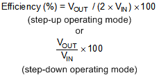
The efficiency of the charge pump regulator varies with the output voltage version, the applied input voltage, the load current, and the internal operation mode of the device.
The approximate efficiency is given by:

Table 1. Operating Mode Change versus VIN
| PRODUCT | OPERATING MODE CHANGES AT VIN OF |
|---|---|
| REG710-2.5 | > 3.2 V |
| REG710-2.7 | > 3.4 V |
| REG710-3 | > 3.7 V |
| REG710-3.3 | > 4.0 V |
| REG710-5, REG71050, REG71055 | Step-up only |
Table 1 lists the approximate values of the input voltage at which the device changes internal operating mode. See efficiency curves in Typical Characteristics for various loads and input voltages.