SLVS077F April 1977 – January 2021 SG2524 , SG3524
PRODUCTION DATA
- 1 Features
- 2 Applications
- 3 Description
- 4 Revision History
- 5 Pin Configurations and Functions
- 6 Specifications
- 7 12
- 8 Parameter Measurement Information
- 9 Detailed Description
- 10Layout
- 11Device and Documentation Support
Package Options
Refer to the PDF data sheet for device specific package drawings
Mechanical Data (Package|Pins)
- NS|16
- N|16
- D|16
Thermal pad, mechanical data (Package|Pins)
Orderable Information
3 Description
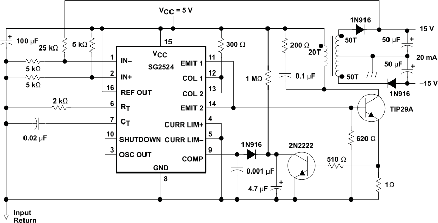
The SG2524 and SG3524 devices incorporate all the functions required in the construction of a regulating power supply, inverter, or switching regulator on a single chip. They also can be used as the control element for high-power-output applications. The SG2524 and SG3524 were designed for switching regulators of either polarity, transformer-coupled dc-to-dc converters, transformerless voltage doublers, and polarity-converter applications employing fixed-frequency, pulse-width modulation (PWM) techniques. The complementary output allows either single-ended or push-pull application. Each device includes an on-chip regulator, error amplifier, programmable oscillator, pulse-steering flip-flop, two uncommitted pass transistors, a high-gain comparator, and current-limiting and shutdown circuitry.
| PART NUMBER | PACKAGE (PIN) | BODY SIZE (NOM) |
|---|---|---|
| SGx524 | SOIC (16) | 9.90 mm × 3.91 mm |
| PDIP (16) | 9.90 mm × 6.35 mm | |
| NS (16) | 10.30 mm × 5.30 mm |
 Typical Application Schematic