SPNS155I September 2009 – June 2015 SM470R1B1M-HT
PRODUCTION DATA.
- 1 Device Overview
- 2 Revision History
- 3 Device Characteristics
- 4 Bare Die
- 5 Pin Configuration and Functions
-
6 Specifications
- 6.1 Absolute Maximum Ratings
- 6.2 ESD Ratings
- 6.3 Recommended Operating Conditions
- 6.4 Electrical Characteristics
- 6.5 Thermal Characteristics
- 6.6 ZPLL and Clock Specifications
- 6.7 RST and PORRST Timings
- 6.8 JTAG Scan Interface Timing
- 6.9 Output Timings
- 6.10 Input Timings
- 6.11 Flash Timings
- 6.12 SPIn Master Mode Timing Parameters
- 6.13 SPIn Slave Mode Timing Parameters
- 6.14 SCIN Isosynchronous Mode Timings - Internal Clock
- 6.15 SCIN Isosynchronous Mode Timings - External Clock
- 6.16 I2C Timing
- 6.17 Standard Can Controller (SCC) Mode Timings
- 6.18 Expansion Bus Module Timing
- 6.19 Multi-Buffered A-to-D Converter (MibADC)
- 7 Parameter Measurement Information
- 8 Detailed Description
- 9 Device and Documentation Support
- 10Mechanical Packaging and Orderable Information
6 Specifications
6.1 Absolute Maximum Ratings
over operating free-air temperature range, A version (unless otherwise noted)(1)| MIN | MAX | UNIT | ||
|---|---|---|---|---|
| Supply voltage | VCC(2) | –0.3 | 2.5 | V |
| Supply voltage | VCCIO, VCCAD, VCCP (flash pump)(2) | –0.3 | 4.1 | V |
| Input voltage | All 5-V tolerant input pins | –0.3 | 6.0 | V |
| All other input pins | –0.3 | 4.1 | V | |
| Input clamp current | IIK (VI < 0 or VI > VCCIO) All pins except ADIN[0:11], PORRST, TRST, TEST, and TCK |
±20 | mA | |
| IIK (VI < 0 or VI > VCCAD) ADIN[0:11] |
±10 | mA | ||
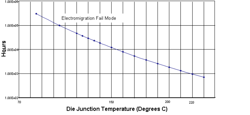
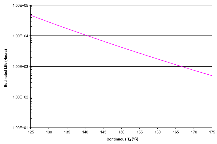
| Operating free-air temperature, TA | HFQ/HKP package | –55 | 220 | °C |
| PGE package | –55 | 150 | °C | |
| Storage temperature, Tstg | –55 | 220 | °C | |
6.2 ESD Ratings
| VALUE | UNIT | |||
|---|---|---|---|---|
| SM470R1B1M-HT in CFP Package | ||||
| V(ESD) | Electrostatic discharge | Human-body model (HBM), per ANSI/ESDA/JEDEC JS-001(1) | 2000 | V |
| Charged-device model (CDM), per JEDEC specification JESD22-C101(2) | 750 | |||
| SM470R1B1M-HT in LQFP Package | ||||
| V(ESD) | Electrostatic discharge | Human-body model (HBM), per ANSI/ESDA/JEDEC JS-001(1) | 2000 | V |
| Charged-device model (CDM), per JEDEC specification JESD22-C101(2) | 750 | |||
6.3 Recommended Operating Conditions(1)
| MIN | NOM | MAX | UNIT | |||
|---|---|---|---|---|---|---|
| VCC | Digital logic supply voltage (Core) | SYSCLK = 48 MHz (pipeline mode enabled) |
1.71 | 2.05 | V | |
| SYSCLK = 60 MHz (pipeline mode enabled) |
1.81 | 2.05 | ||||
| VCCIO | Digital logic supply voltage (I/O) | 3 | 3.6 | V | ||
| VCCAD | ADC supply voltage | 3 | 3.6 | V | ||
| VCCP | Flash pump supply voltage | 3 | 3.6 | V | ||
| VSS | Digital logic supply ground | 0 | V | |||
| VSSAD | ADC supply ground(1) | –0.1 | 0.1 | V | ||
| TA | Operating free-air temperature | HFQ/HKP package | –55 | 220 | °C | |
| PGE package | –55 | 150 | ||||
6.4 Electrical Characteristics
Minimum and maximum parameters are characterized over the operating temperature range unless otherwise noted, but may not be production tested at that temperature. Production test limits with statistical guardbands are used to ensure high temperature performance. (1)| PARAMETER | TEST CONDITIONS | MIN | TYP(2) | MAX | UNIT | ||
|---|---|---|---|---|---|---|---|
| Vhys | Input hysteresis | 0.15 | V | ||||
| VIL | Low-level input voltage |
All inputs(3) | –0 .3 | 0.8 | V | ||
| VIH | High-level input voltage |
All inputs | 2 | VCCIO + 0. 3 | V | ||
| Input threshold voltage |
AWD only(4) | 1.35 | 1.8 | ||||
| OSCIN with digital input only | 0.7 VCC | VCC + 0.3 | |||||
| VOL | Low-level output voltage(5) | IOL = IOL MAX | 0.2 VCCIO | V | |||
| IOL = 50 µA | 0.2 | ||||||
| VOH | High-level output voltage(5) | IOH = IOH MIN | 0.8 VCCIO | V | |||
| IOH = 50 µA | VCCIO – 0.2 | ||||||
| IIC | Input clamp current (I/O pins)(6) | VI < VSSIO – 0. 3 or VI > VCCIO + 0. 3 |
–2 | 2 | mA | ||
| II | Input current (3.3 V input pins) |
IIL Pulldown | VI = VSS | –1 | 1 | µA | |
| IIH Pulldown | VI = VCCIO | 5 | 100 | ||||
| IIL Pullup | VI = VSS | –100 | –5 | ||||
| IIH Pullup | VI = VCCIO | –1 | 1 | ||||
| All other pins | No pullup or pulldown | –1 | 1 | ||||
| Input current (5 V tolerant input pins) | VI = VSS | –1 | 1 | µA | |||
| VI = VCCIO | 1 | 5 | |||||
| VI = 5 V | 5 | 25 | |||||
| VI = 5.5 V | 25 | 50 | |||||
| IOL | Low-level output current |
CLKOUT, AWD, TDI, TDO, TMS, TMS2 | VOL = VOL MAX | 8 | mA | ||
| RST | 4 | ||||||
| All other 3.3 V I/O(7) | 2 | ||||||
| 5 V tolerant | 4 | ||||||
| IOH | High-level output current |
CLKOUT, TDI, TDO, TMS, TMS2 | VOH = VOH MIN | –8 | mA | ||
| RST | –4 | ||||||
| All other 3.3 V I/O(7) | –2 | ||||||
| 5 V tolerant | –4 | ||||||
| ICC | VCC Digital supply current (operating mode) | SYSCLK = 48 MHz, ICLK = 24 MHz, VCC = 2.05 V |
110 | mA | |||
| SYSCLK = 60 MHz, ICLK = 30 MHz, VCC = 2.05 V |
125 | mA | |||||
| VCC Digital supply current (standby mode)(8)(9) | OSCIN = 5 MHz, VCC = 2.05 V | 28 | mA | ||||
| VCC Digital supply current (halt mode)(8)(9) | All frequencies, VCC = 2.05 V | 700 | µA | ||||
| ICCIO | VCCIO Digital supply current (operating mode) | No DC load, VCCIO = 3.6 V(10) | 20 | mA | |||
| VCCIO Digital supply current (standby mode)(9) | No DC load, VCCIO = 3.6 V(10) | 250 | µA | ||||
| VCCIO Digital supply current (halt mode)(9) | No DC load, VCCIO = 3.6 V(10) | 225 | µA | ||||
| ICCAD | VCCAD supply current (operating mode) | All frequencies, VCCAD = 3.6 V | 15 | mA | |||
| VCCAD supply current (standby mode) | All frequencies, VCCAD = 3.6 V | 10 | µA | ||||
| VCCAD supply current (halt mode) | All frequencies, VCCAD = 3.6 V | 10 | µA | ||||
| ICCP | VCCP pump supply current | SYSCLK = 48 MHz, VCCP = 3.6 V read operation | 45 | mA | |||
| SYSCLK = 60 MHz, VCCP = 3.6 V read operation | 55 | mA | |||||
| VCCP = 3.6 V program and erase | 70 | mA | |||||
| VCCP = 3.6 V standby mode operation(8) | 10 | µA | |||||
| VCCP = 3.6 V halt mode operation(8) | 10 | µA | |||||
| CI | Input capacitance | 2 | pF | ||||
| CO | Output capacitance | 3 | pF | ||||
6.5 Thermal Characteristics
| THERMAL METRIC(1) | SM470R1B1M-HT | UNIT | ||
|---|---|---|---|---|
| HFQ (CQFP) OR HKP (CFP) | PGE (LQFP) | |||
| 64 PINS | 144 PINS | |||
| RθJA | Junction-to-ambient thermal resistance | N/A | 38.3 | °C/W |
| RθJC(top) | Junction-to-case (top) thermal resistance | N/A | 5.7 | °C/W |
| RθJB | Junction-to-board thermal resistance | 152.0148 | 19.7 | °C/W |
| ψJT | Junction-to-top characterization parameter | N/A | 0.1 | °C/W |
| ψJB | Junction-to-board characterization parameter | N/A | 19.3 | °C/W |
| RθJC(bot) | Junction-to-case (bottom) thermal resistance | 5.4898 | N/A | °C/W |
6.6 ZPLL and Clock Specifications
Table 6-1 Timing Requirements for ZPLL Circuits Enabled or Disabled(1)
| MIN | TYP | MAX | UNIT | ||
|---|---|---|---|---|---|
| ƒ(OSC) | Input clock frequency | 4 | 10 | MHz | |
| tc(OSC) | Cycle time, OSCIN | 100 | ns | ||
| tw(OSCIL) | Pulse duration, OSCIN low | 15 | ns | ||
| tw(OSCIH) | Pulse duration, OSCIN high | 15 | ns | ||
| ƒ(OSCRST) | OSC FAIL frequency(2) | 53 | kHz | ||
Table 6-2 Switching Characteristics over Recommended Operating Conditions for Clocks(1)(2)(3)(4)
| PARAMETER | TEST CONDITIONS(5) | MIN | MAX | UNIT | |
|---|---|---|---|---|---|
| ƒ(SYS) | System clock frequency(6) | Pipeline mode enabled | 60(7) | MHz | |
| Pipeline mode disabled | 24 | MHz | |||
| ƒ(CONFIG) | System clock frequency - flash config mode | 24 | MHz | ||
| ƒ(ICLK) | Interface clock frequency | Pipeline mode enabled | 30 | MHz | |
| Pipeline mode disabled | 24 | MHz | |||
| ƒ(ECLK) | External clock output frequency for ECP module | Pipeline mode enabled | 30 | MHz | |
| Pipeline mode disabled | 24 | MHz | |||
| tc(SYS) | Cycle time, system clock | Pipeline mode enabled | 16.7 | ns | |
| Pipeline mode disabled | 41.6 | ns | |||
| tc(CONFIG) | Cycle time, system clock - flash config mode | 41.6 | ns | ||
| tc(ICLK) | Cycle time, interface clock | Pipeline mode enabled | 33.3 | ns | |
| Pipeline mode disabled | 41.6 | ns | |||
| tc(ECLK) | Cycle time, ECP module external clock output | Pipeline mode enabled | 33.3 | ns | |
| Pipeline mode disabled | 41.6 | ns | |||
ƒ(SYS) = ƒ(OSC)/R, where R = {1,2,3,4,5,6,7,8} when PLLDIS = 1.
ƒ(ICLK) = ƒ(SYS)/X, where X = {1,2,3,4,5,6,7,8,9,10,11,12,13,14,15,16}. X is the interface clock divider ratio determined by the PCR0[4:1] bits in the SYS module.
Table 6-3 Switching Characteristics over Recommended Operating Conditions for External Clocks(1)(2)(3)(4)
(see Figure 6-3 and Figure 6-4)| PARAMETER | TEST CONDITIONS | MIN | MAX | UNIT | |
|---|---|---|---|---|---|
| tw(COL) | Pulse duration, CLKOUT low | SYSCLK or MCLK(5) | 0.5tc(SYS) – tf | ns | |
| ICLK: X is even or 1(6) | 0.5tc(ICLK) – tf | ||||
| ICLK: X is odd and not 1(6) | 0.5tc(ICLK) + 0.5tc(SYS) – tf | ||||
| tw(COH) | Pulse duration, CLKOUT high | SYSCLK or MCLK(5) | 0.5tc(SYS) – tr | ns | |
| ICLK: X is even or 1(6) | 0.5tc(ICLK) – tr | ||||
| ICLK: X is odd and not 1(6) | 0.5tc(ICLK) – 0.5tc(SYS) – tr | ||||
| tw(EOL) | Pulse duration, ECLK low | N is even and X is even or odd | 0.5tc(ECLK) – tf | ns | |
| N is odd and X is even | 0.5tc(ECLK) – tf | ||||
| N is odd and X is odd and not 1 | 0.5tc(ECLK) + 0.5tc(SYS) – tf | ||||
| tw(EOH) | Pulse duration, ECLK high | N is even and X is even or odd | 0.5tc(ECLK) – tr | ns | |
| N is odd and X is even | 0.5tc(ECLK) – tr | ||||
| N is odd and X is odd and not 1 | 0.5tc(ECLK) – 0.5tc(SYS) – tr | ||||
 Figure 6-3 CLKOUT Timing Diagram
 Figure 6-4 ECLK Timing Diagram
6.7 RST and PORRST Timings
Table 6-4 Timing Requirements for PORRST(1)
(see Figure 6-5)| MIN | MAX | UNIT | ||
|---|---|---|---|---|
| VCCPORL | VCC low supply level when PORRST must be active during power up | 0.6 | V | |
| VCCPORH | VCC high supply level when PORRST must remain active during power up and become active during power down | 1.5 | V | |
| VCCIOPORL | VCCIO low supply level when PORRST must be active during power up | 1.1 | V | |
| VCCIOPORH | VCCIO high supply level when PORRST must remain active during power up and become active during power down | 2.75 | V | |
| VIL | Low-level input voltage after VCCIO > VCCIOPORH | 0.2 VCCIO | V | |
| VIL(PORRST) | Low-level input voltage of PORRST before VCCIO > VCCIOPORL | 0.5 | V | |
| tsu(PORRST)r | Setup time, PORRST active before VCCIO > VCCIOPORL during power up | 0 | ms | |
| tsu(VCCIO)r | Setup time, VCCIO > VCCIOPORL before VCC > VCCPORL | 0 | ms | |
| th(PORRST)r | Hold time, PORRST active after VCC > VCCPORH | 1 | ms | |
| tsu(PORRST)f | Setup time, PORRST active before VCC ≤ VCCPORH during power down | 8 | µs | |
| th(PORRST)rio | Hold time, PORRST active after VCC > VCCIOPORH | 1 | ms | |
| th(PORRST)d | Hold time, PORRST active after VCC < VCCPORL | 0 | ms | |
| tsu(PORRST)fio | Setup time, PORRST active before VCC ≤ VCCIOPORH during power down | 0 | ns | |
| tsu(VCCIO)f | Setup time, VCC < VCCPORL before VCCIO < VCCIOPORL | 0 | ns | |

Table 6-5 Switching Characteristics over Recommended Operating Conditions for RST(1)(2)
| PARAMETER | MIN | MAX | UNIT | |
|---|---|---|---|---|
| tv(RST) | Valid time, RST active after PORRST inactive | 4112tc(OSC) | ns | |
| Valid time, RST active (all others) | 8tc(SYS) | |||
| tfsu | Flash start up time, from RST inactive to fetch of first instruction from flash (flash pump stabilization time) | 836tc(OSC) | ns | |
6.8 JTAG Scan Interface Timing
Table 6-6 JTAG Clock Specification 10-MHz and 50-pF Load on TDO Output(1)
| MIN | MAX | UNIT | ||
|---|---|---|---|---|
| tc(JTAG) | Cycle time, JTAG low and high period | 50 | ns | |
| tsu(TDI/TMS - TCKr) | Setup time, TDI, TMS before TCK rise (TCKr) | 15 | ns | |
| th(TCKr -TDI/TMS) | Hold time, TDI, TMS after TCKr | 15 | ns | |
| th(TCKf -TDO) | Hold time, TDO after TCKf | 10 | ns | |
| td(TCKf -TDO) | Delay time, TDO valid after TCK fall (TCKf) | 45 | ns | |
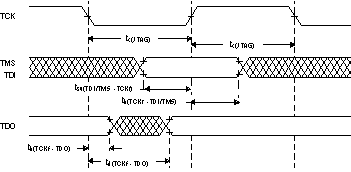 Figure 6-6 JTAG Scan Timings
6.9 Output Timings
Table 6-7 Switching Characteristics for Output Timings versus Load Capacitance (CL)(1)
(see Figure 6-7)| PARAMETER | MIN | MAX | UNIT | ||
|---|---|---|---|---|---|
| tr | Rise time, AWD, CLKOUT, TDI, TDO, TMS, TMS2 | CL = 15 pF | 0.5 | 2.5 | ns |
| CL = 50 pF | 1.5 | 5.0 | |||
| CL = 100 pF | 3.0 | 9.0 | |||
| CL = 150 pF | 4.5 | 12.5 | |||
| tf | Fall time, AWD, CLKOUT, TDI, TDO, TMS, TMS2 | CL = 15 pF | 0.5 | 2.5 | ns |
| CL = 50 pF | 1.5 | 5.0 | |||
| CL = 100 pF | 3.0 | 9.0 | |||
| CL = 150 pF | 4.5 | 12.5 | |||
| tr | Rise time, RST | CL = 15 pF | 2.5 | 8 | ns |
| CL = 50 pF | 5 | 14 | |||
| CL = 100 pF | 9 | 23 | |||
| CL = 150 pF | 13 | 32 | |||
| tr | Rise time, 4-mA, 5-V tolerant pins | CL = 15 pF | 3 | 10 | ns |
| CL = 50 pF | 3.5 | 12 | |||
| CL = 100 pF | 7 | 21 | |||
| CL = 150 pF | 9 | 28 | |||
| CL = 400 pF | 18 | 40 | |||
| tf | Fall time, 4-mA, 5-V tolerant pins | CL = 15 pF | 2 | 8 | ns |
| CL = 50 pF | 2.5 | 9 | |||
| CL = 100 pF | 8 | 25 | |||
| CL = 150 pF | 11 | 35 | |||
| CL = 400 pF | 20 | 45 | |||
| tr | Rise time, all other output pins | CL = 15 pF | 2.5 | 10 | ns |
| CL = 50 pF | 6.0 | 25 | |||
| CL = 100 pF | 12 | 45 | |||
| CL = 150 pF | 18 | 65 | |||
| tf | Fall time, all other output pins | CL = 15 pF | 3 | 10 | ns |
| CL = 50 pF | 8.5 | 25 | |||
| CL = 100 pF | 16 | 45 | |||
| CL = 150 pF | 23 | 65 | |||
 Figure 6-7 CMOS-Level Outputs
6.10 Input Timings
Table 6-8 Timing Requirements for Input Timings(1)(2)
(see Figure 6-8)| MIN | MAX | UNIT | ||
|---|---|---|---|---|
| tpw | Input minimum pulse width | tc(ICLK) + 10 | ns | |
 Figure 6-8 CMOS-Level Inputs
6.11 Flash Timings
Table 6-9 Timing Requirements for Program Flash(1)(2)
| MIN | TYP | MAX | UNIT | ||
|---|---|---|---|---|---|
| tprog(16-bit) | Half word (16-bit) programming time | 4 | 16 | 200 | µs |
| tprog(Total) | 1MB programming time(3) | 8 | 32 | s | |
| terase(sector) | Sector erase time, TA = –40°C to 150°C | 1.7 | s | ||
| twec | Write/erase cycles at TA = –40°C to 85°C | 50000 | cycles | ||
| tfp(RST) | Flash pump settling time from RST to SLEEP | 167tc(SYS) | ns | ||
| tfp(SLEEP) | Initial flash pump settling time from SLEEP to STANDBY | 167tc(SYS) | ns | ||
| tfp(STANDBY) | Initial flash pump settling time from STANDBY to ACTIVE | 84tc(SYS) | ns | ||
6.12 SPIn Master Mode Timing Parameters
Table 6-10 SPIn Master Mode External Timing Parameters
(CLOCK PHASE = 0, SPInCLK = output, SPInSIMO = output, and SPInSOMI = input)(1)(2)(3)(4) (see Figure 6-9)| NO. | MIN | MAX | UNIT | ||
|---|---|---|---|---|---|
| 1 | tc(SPC)M | Cycle time, SPInCLK(5) | 100 | 256tc(ICLK) | ns |
| 2(6) | tw(SPCH)M | Pulse duration, SPInCLK high (clock polarity = 0) | 0.5tc(SPC)M – tr | 0.5tc(SPC)M + 5 | |
| tw(SPCL)M | Pulse duration, SPInCLK low (clock polarity = 1) | 0.5tc(SPC)M – tf | 0.5tc(SPC)M + 5 | ||
| 3(6) | tw(SPCL)M | Pulse duration, SPInCLK low (clock polarity = 0) | 0.5tc(SPC)M – tf | 0.5tc(SPC)M + 5 | |
| tw(SPCH)M | Pulse duration, SPInCLK high (clock polarity = 1) | 0.5tc(SPC)M – tr | 0.5tc(SPC)M + 5 | ||
| 4(6) | td(SPCH-SIMO)M | Delay time, SPInCLK high to SPInSIMO valid (clock polarity = 0) | 10 | ||
| td(SPCL-SIMO)M | Delay time, SPInCLK low to SPInSIMO valid (clock polarity = 1) | 10 | |||
| 5(6) | tv(SPCL-SIMO)M | Valid time, SPInSIMO data valid after SPInCLK low (clock polarity = 0) | tc(SPC)M – 5 – tf | ||
| tv(SPCH-SIMO)M | Valid time, SPInSIMO data valid after SPInCLK high (clock polarity = 1) | tc(SPC)M – 5 – tr | |||
| 6(6) | tsu(SOMI-SPCL)M | Setup time, SPInSOMI before SPInCLK low (clock polarity = 0) | 6 | ||
| tsu(SOMI-SPCH)M | Setup time, SPInSOMI before SPInCLK high (clock polarity = 1) | 6 | |||
| 7(6) | tv(SPCL-SOMI)M | Valid time, SPInSOMI data valid after SPInCLK low (clock polarity = 0) | 4 | ||
| tv(SPCH-SOMI)M | Valid time, SPInSOMI data valid after SPInCLK high (clock polarity = 1) | 4 | |||
For PS values from 1 to 255: t c(SPC)M ≥(PS +1)tc(ICLK) ≥ 100 ns, where PS is the prescale value set in the SPInCTL1[12:5] register bits.
For PS values of 0: tc(SPC)M = 2t c(ICLK) ≥ 100 ns.
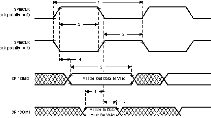 Figure 6-9 SPIn Master Mode External Timing (CLOCK PHASE = 0)
Table 6-11 SPIn Master Mode External Timing Parameters(1)
(CLOCK PHASE = 1, SPInCLK = output, SPInSIMO = output, and SPInSOMI = input)(2)(3)(4) (see Figure 6-10)| NO. | MIN | MAX | UNIT | ||
|---|---|---|---|---|---|
| 1 | tc(SPC)M | Cycle time, SPInCLK(5) | 100 | 256tc(ICLK) | ns |
| 2(6) | tw(SPCH)M | Pulse duration, SPInCLK high (clock polarity = 0) | 0.5tc(SPC)M – tr | 0.5tc(SPC)M + 5 | |
| tw(SPCL)M | Pulse duration, SPInCLK low (clock polarity = 1) | 0.5tc(SPC)M – tf | 0.5tc(SPC)M + 5 | ||
| 3(6) | tw(SPCL)M | Pulse duration, SPInCLK low (clock polarity = 0) | 0.5tc(SPC)M – tf | 0.5tc(SPC)M + 5 | |
| tw(SPCH)M | Pulse duration, SPInCLK high (clock polarity = 1) | 0.5tc(SPC)M – tr | 0.5tc(SPC)M + 5 | ||
| 4(6) | tv(SIMO-SPCH)M | Valid time, SPInCLK high after SPInSIMO data valid (clock polarity = 0) |
0.5tc(SPC)M – 10 | ||
| tv(SIMO-SPCL)M | Valid time, SPInCLK low after SPInSIMO data valid (clock polarity = 1) |
0.5tc(SPC)M – 10 | |||
| 5(6) | tv(SPCH-SIMO)M | Valid time, SPInSIMO data valid after SPInCLK high (clock polarity = 0) |
0.5tc(SPC)M – 5 – tr | ||
| tv(SPCL-SIMO)M | Valid time, SPInSIMO data valid after SPInCLK low (clock polarity = 1) |
0.5tc(SPC)M – 5 – tf | |||
| 6(6) | tsu(SOMI-SPCH)M | Setup time, SPInSOMI before SPInCLK high (clock polarity = 0) |
6 | ||
| tsu(SOMI-SPCL)M | Setup time, SPInSOMI before SPInCLK low (clock polarity = 1) |
6 | |||
| 7(6) | tv(SPCH-SOMI)M | Valid time, SPInSOMI data valid after SPInCLK high (clock polarity = 0) |
4 | ||
| tv(SPCL-SOMI)M | Valid time, SPInSOMI data valid after SPInCLK low (clock polarity = 1) |
4 | |||
For PS values from 1 to 255: t c(SPC)M ≥ (PS +1)tc(ICLK) ≥ 100 ns, where PS is the prescale value set in the SPInCTL1[12:5] register bits.
For PS values of 0: tc(SPC)M = 2t c(ICLK) ≥ 100 ns.
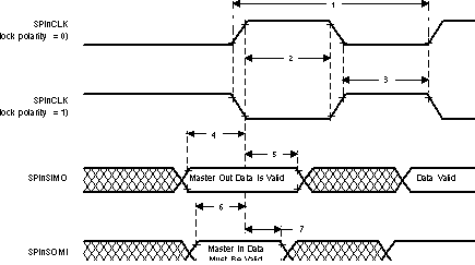 Figure 6-10 SPIn Master Mode External Timing (CLOCK PHASE = 1)
6.13 SPIn Slave Mode Timing Parameters
Table 6-12 SPIn Slave Mode External Timing Parameters(1)
(CLOCK PHASE = 0, SPInCLK = input, SPInSIMO = input, and SPInSOMI = output)(2)(3)(4)(5) (see Figure 6-11)| NO. | MIN | MAX | UNIT | ||
|---|---|---|---|---|---|
| 1 | tc(SPC)S | Cycle time, SPInCLK(6) | 100 | 256tc(ICLK) | ns |
| 2(7) | tw(SPCH)S | Pulse duration, SPInCLK high (clock polarity = 0) | 0.5tc(SPC)S – 0.25tc(ICLK) | 0.5tc(SPC)S + 0.25tc(ICLK) | |
| tw(SPCL)S | Pulse duration, SPInCLK low (clock polarity = 1) | 0.5tc(SPC)S – 0.25tc(ICLK) | 0.5tc(SPC)S + 0.25tc(ICLK) | ||
| 3(7) | tw(SPCL)S | Pulse duration, SPInCLK low (clock polarity = 0) | 0.5tc(SPC)S – 0.25tc(ICLK) | 0.5tc(SPC)S + 0.25tc(ICLK) | |
| tw(SPCH)S | Pulse duration, SPInCLK high (clock polarity = 1) | 0.5tc(SPC)S – 0.25tc(ICLK) | 0.5tc(SPC)S + 0.25tc(ICLK) | ||
| 4(7) | td(SPCH-SOMI)S | Delay time, SPInCLK high to SPInSOMI valid (clock polarity = 0) |
6 + tr | ||
| td(SPCL-SOMI)S | Delay time, SPInCLK low to SPInSOMI valid (clock polarity = 1) |
6 + tf | |||
| 5(7) | tv(SPCH-SOMI)S | Valid time, SPInSOMI data valid after SPInCLK high (clock polarity = 0) |
tc(SPC)S – 6 – tr | ||
| tv(SPCL-SOMI)S | Valid time, SPInSOMI data valid after SPInCLK low (clock polarity = 1) |
tc(SPC)S – 6 – tf | |||
| 6(7) | tsu(SIMO-SPCL)S | Setup time, SPInSIMO before SPInCLK low (clock polarity = 0) |
6 | ||
| tsu(SIMO-SPCH)S | Setup time, SPInSIMO before SPInCLK high (clock polarity = 1) |
6 | |||
| 7(7) | tv(SPCL-SIMO)S | Valid time, SPInSIMO data valid after SPInCLK low (clock polarity = 0) |
6 | ||
| tv(SPCH-SIMO)S | Valid time, SPInSIMO data valid after SPInCLK high (clock polarity = 1) |
6 | |||
For PS values from 1 to 255: t c(SPC)S ≥ (PS +1)tc(ICLK) ≥ 100 ns, where PS is the prescale value set in the SPInCTL1[12:5] register bits.
For PS values of 0: tc(SPC)S = 2t c(ICLK) ≥ 100 ns.
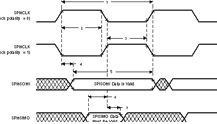 Figure 6-11 SPIn Slave Mode External Timing (CLOCK PHASE = 0)
Table 6-13 SPIn Slave Mode External Timing Parameters(1)
(CLOCK PHASE = 1, SPInCLK = input, SPInSIMO = input, and SPInSOMI = output)(2)(3)(4)(5) (see Figure 6-12)| NO. | MIN | MAX | UNIT | ||
|---|---|---|---|---|---|
| 1 | tc(SPC)S | Cycle time, SPInCLK(6) | 100 | 256tc(ICLK) | ns |
| 2(7) | tw(SPCH)S | Pulse duration, SPInCLK high (clock polarity = 0) | 0.5tc(SPC)S – 0.25tc(ICLK) | 0.5tc(SPC)S + 0.25tc(ICLK) | |
| tw(SPCL)S | Pulse duration, SPInCLK low (clock polarity = 1) | 0.5tc(SPC)S – 0.25tc(ICLK) | 0.5tc(SPC)S + 0.25tc(ICLK) | ||
| 3(7) | tw(SPCL)S | Pulse duration, SPInCLK low (clock polarity = 0) | 0.5tc(SPC)S – 0.25tc(ICLK) | 0.5tc(SPC)S + 0.25tc(ICLK) | |
| tw(SPCH)S | Pulse duration, SPInCLK high (clock polarity = 1) | 0.5tc(SPC)S – 0.25tc(ICLK) | 0.5tc(SPC)S + 0.25tc(ICLK) | ||
| 4(7) | tv(SOMI-SPCH)S | Valid time, SPInCLK high after SPInSOMI data valid (clock polarity = 0) |
0.5tc(SPC)S – 6 – tr | ||
| tv(SOMI-SPCL)S | Valid time, SPInCLK low after SPInSOMI data valid (clock polarity = 1) |
0.5tc(SPC)S – 6 – tf | |||
| 5(7) | tv(SPCH-SOMI)S | Valid time, SPInSOMI data valid after SPInCLK high (clock polarity = 0) |
0.5tc(SPC)S – 6 – tr | ||
| tv(SPCL-SOMI)S | Valid time, SPInSOMI data valid after SPInCLK low (clock polarity = 1) |
0.5tc(SPC)S – 6 – tf | |||
| 6(7) | tsu(SIMO-SPCH)S | Setup time, SPInSIMO before SPInCLK high (clock polarity = 0) |
6 | ||
| tsu(SIMO-SPCL)S | Setup time, SPInSIMO before SPInCLK low (clock polarity = 1) |
6 | |||
| 7(7) | tv(SPCH-SIMO)S | Valid time, SPInSIMO data valid after SPInCLK high (clock polarity = 0) |
6 | ||
| tv(SPCL-SIMO)S | Valid time, SPInSIMO data valid after SPInCLK low (clock polarity = 1) |
6 | |||
For PS values from 1 to 255: t c(SPC)S ≥ (PS +1)tc(ICLK) ≥ 100 ns, where PS is the prescale value set in the SPInCTL1[12:5] register bits.
For PS values of 0: tc(SPC)S = 2t c(ICLK) ≥ 100 ns.
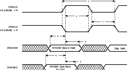 Figure 6-12 SPIn Slave Mode External Timing (CLOCK PHASE = 1)
6.14 SCIN Isosynchronous Mode Timings - Internal Clock
Table 6-14 Timing Requirements for Internal Clock SCIN Isosynchronous Mode(1)(2)(3)(4)
(see Figure 6-13)| (BAUD + 1) IS EVEN OR BAUD = 0 |
(BAUD + 1) IS ODD AND BAUD ≠ 0 |
UNIT | ||||
|---|---|---|---|---|---|---|
| MIN | MAX | MIN | MAX | |||
| tc(SCC) | Cycle time, SCInCLK | 2tc(ICLK) | 224 tc(ICLK) | 3tc(ICLK) | (224 – 1) tc(ICLK) | ns |
| tw(SCCL) | Pulse duration, SCInCLK low | 0.5tc(SCC) – tf | 0.5tc(SCC) + 5 | 0.5tc(SCC) + 0.5tc(ICLK) – tf | 0.5tc(SCC) + 0.5tc(ICLK) | ns |
| tw(SCCH) | Pulse duration, SCInCLK high | 0.5tc(SCC) – tr | 0.5tc(SCC) + 5 | 0.5tc(SCC) – 0.5tc(ICLK) – tr | 0.5tc(SCC) – 0.5tc(ICLK) | ns |
| td(SCCH-TXV) | Delay time, SCInCLK high to SCInTX valid | 10 | 10 | ns | ||
| tv(TX) | Valid time, SCInTX data after SCInCLK low | tc(SCC) – 10 | tc(SCC) – 10 | ns | ||
| tsu(RX-SCCL) | Setup time, SCInRX before SCInCLK low | tc(ICLK) + tf + 20 | tc(ICLK) + tf + 20 | ns | ||
| tv(SCCL-RX) | Valid time, SCInRX data after SCInCLK low | –tc(ICLK) + tf + 20 | –tc(ICLK) + tf + 20 | ns | ||

NOTE:
Data transmission/reception characteristics for isosynchronous mode with internal clocking are similar to the asynchronous mode. Data transmission occurs on the SCICLK rising edge, and data reception occurs on the SCICLK falling edge.6.15 SCIN Isosynchronous Mode Timings - External Clock
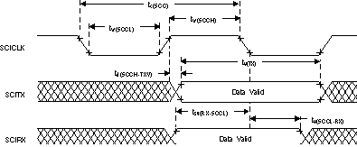
Table 6-15 Timing Requirements for External Clock SCIN Isosynchronous Mode(1)(2)(3)
(see Figure 6-14)| MIN | MAX | UNIT | ||
|---|---|---|---|---|
| tc(SCC) | Cycle time, SCInCLK(4) | 8tc(ICLK) | ns | |
| tw(SCCH) | Pulse duration, SCInCLK high | 0.5tc(SCC) – 0.25tc(ICLK) | 0.5tc(SCC) + 0.25tc(ICLK) | ns |
| tw(SCCL) | Pulse duration, SCInCLK low | 0.5tc(SCC) – 0.25tc(ICLK) | 0.5tc(SCC) + 0.25tc(ICLK) | ns |
| td(SCCH-TXV) | Delay time, SCInCLK high to SCInTX valid | 2tc(ICLK) + 12 + t r | ns | |
| tv(TX) | Valid time, SCInTX data after SCInCLK low | 2tc(SCC) – 10 | ns | |
| tsu(RX-SCCL) | Setup time, SCInRX before SCInCLK low | 0 | ns | |
| tv(SCCL-RX) | Valid time, SCInRX data after SCInCLK low | 2tc(ICLK) + 10 | ns | |
6.16 I2C Timing
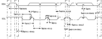
Table 6-16 Assumes testing over recommended operating conditions.
Table 6-16 I2C Signals (SDA and SCL) Switching Characteristics(1)(2)
| PARAMETER | STANDARD MODE | FAST MODE | UNIT | ||||
|---|---|---|---|---|---|---|---|
| MIN | MAX | MIN | MAX | ||||
| tc(I2CCLK) | Cycle time, I2C module clock | 75 | 150 | 75 | 150 | ns | |
| tc(SCL) | Cycle time, SCL | 10 | 2.5 | µs | |||
| tsu(SCLH-SDAL) | Setup time, SCL high before SDA low (for a repeated START condition) | 4.7 | 0.6 | µs | |||
| th(SCLL-SDAL) | Hold time, SCL low after SDA low (for a repeated START condition) | 4 | 0.6 | µs | |||
| tw(SCLL) | Pulse duration, SCL low | 4.7 | 1.3 | µs | |||
| tw(SCLH) | Pulse duration, SCL high | 4 | 0.6 | µs | |||
| tsu(SDA-SCLH) | Setup time, SDA valid before SCL high | 250 | 100 | ns | |||
| th(SDA-SCLL) | Hold time, SDA valid after SCL low | For I2C bus devices | 0 | 3.45(3) | 0 | 0.9 | µs |
| tw(SDAH) | Pulse duration, SDA high between STOP and START conditions | 4.7 | 1.3 | µs | |||
| tr(SCL) | Rise time, SCL | 1000 | 20+0.1Cb(4) | 300 | ns | ||
| tr(SDA) | Rise time, SDA | 1000 | 20+0.1Cb(4) | 300 | ns | ||
| tf(SCL) | Fall time, SCL | 300 | 20+0.1Cb(4) | 300 | ns | ||
| tf(SDA) | Fall time, SDA | 300 | 20+0.1Cb(4) | 300 | ns | ||
| tsu(SCLH-SDAH) | Setup time, SCL high before SDA high (for STOP condition) | 4.0 | 0.6 | µs | |||
| tw(SP) | Pulse duration, spike (must be suppressed) | 0 | 50 | ns | |||
| Cb(4) | Capacitive load for each bus line | 400 | 400 | pF | |||
6.17 Standard Can Controller (SCC) Mode Timings
Table 6-17 Dynamic Characteristics for the CANSTX and CANSRX Pins(1)
| PARAMETER | MIN | MAX | UNIT | |
|---|---|---|---|---|
| td(CANSTX) | Delay time, transmit shift register to CANSTX pin(2) | 15 | ns | |
| td(CANSRX) | Delay time, CANSRX pin to receive shift register | 5 | ns | |
6.18 Expansion Bus Module Timing
Table 6-18 Expansion Bus Timing Parameters(1)
–55°C ≤ TA ≤ 220°C, 3.0 V ≤ V CC ≤ 3.6 V (see Figure 6-16 and Figure 6-17)| MIN | MAX | UNIT | |||
|---|---|---|---|---|---|
| tc(CO) | Cycle time, CLKOUT | 20.8 | ns | ||
| td(COH-EBADV) | Delay time, CLKOUT high to EBADDR valid | 21.4 | ns | ||
| th(COH-EBADIV) | Hold time, EBADDR invalid after CLKOUT high | 12.4 | ns | ||
| td(COH-EBOE) | Delay time, CLKOUT high to EBOE fall | 11.4 | ns | ||
| th(COH-EBOEH) | Hold time, EBOE rise after CLKOUT high | 11.4 | ns | ||
| td(COL-EBWR) | Delay time, CLKOUT low to write strobe (EBWR) low | 11.3 | ns | ||
| th(COL-EBWRH) | Hold time, EBWR high after CLKOUT low | 11.6 | ns | ||
| tsu(EBRDATV-COH) | Setup time, EBDATA valid before CLKOUT high (READ)(2) | 15.2 | ns | ||
| th(COH-EBRDATIV) | Hold time, EBDATA invalid after CLKOUT high (READ) | (–14.7) | ns | ||
| td(COL-EBWDATV) | Delay time, CLKOUT low to EBDATA valid (WRITE)(3) | 16.1 | ns | ||
| th(COL-EBWDATIV) | Hold time, EBDATA invalid after CLKOUT low (WRITE) | 14.7 | ns | ||
| SECONDARY TIMES | |||||
| td(COH-EBCS0) | Delay, CLKOUT high to EBCS0 fall | 13.6 | ns | ||
| th(COH-EBCS0H) | Hold, EBCS0 rise after CLKOUT high | 13.2 | ns | ||
| tsu(COH-EBHOLDL) | Setup time, EBHOLD low to CLKOUT high(2) | 10.9 | ns | ||
| tsu(COH-EBHOLDH) | Setup time, EBHOLD high to CLKOUT high(2) | 10.5 | ns | ||
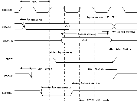 Figure 6-16 Expansion Memory Signal Timing - Reads
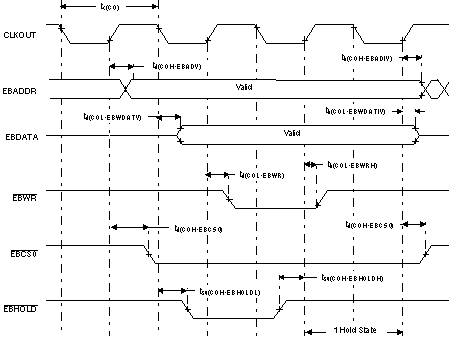 Figure 6-17 Expansion Memory Signal Timing - Writes
6.19 Multi-Buffered A-to-D Converter (MibADC)
The multi-buffered A-to-D converter (MibADC) has a separate power bus for its analog circuitry that enhances the A-to-D performance by preventing digital switching noise on the logic circuitry, which could be present on V SS and V CC , from coupling into the A-to-D analog stage. All A-to-D specifications are given with respect to AD REFLO unless otherwise noted.
| Resolution | 10 bits (1024 values) |
| Monotonic | Assured |
| Output conversion code | 00h to 3FFh [00 for VAI ≤ AD REFLO ; 3FF for VAI ≥ AD REFHI ] |
Table 6-19 MibADC Recommended Operating Conditions(1)
| MIN | MAX | UNIT | ||
|---|---|---|---|---|
| ADREFHI | A-to-D high-voltage reference source | VSSAD | VCCAD | V |
| ADREFLO | A-to-D low-voltage reference source | VSSAD | VCCAD | V |
| VAI | Analog input voltage | VSSAD – 0.3 | VCCAD + 0.3 | V |
| IAIC | Analog input clamp current(2)
(VAI < VSSAD – 0.3 or VAI > VCCAD + 0.3) |
–2 | 2 | mA |
Table 6-20 Operating Characteristics over Full Ranges of Recommended Operating Conditions(1)(2)(3)(4)
| PARAMETER | DESCRIPTION/CONDITIONS | MIN | TYP | MAX | UNIT | ||
|---|---|---|---|---|---|---|---|
| RI | Analog input resistance | See Figure 6-18. | 250 | 500 | Ω | ||
| CI | Analog input capacitance | See Figure 6-18. | Conversion | 10 | pF | ||
| Sampling | 30 | pF | |||||
| IAIL | Analog input leakage current | See Figure 6-18. | –1 | 1 | µA | ||
| IADREFHI | ADREFHI input current | ADREFHI = 3.6 V, ADREFLO = VSSAD | 5 | mA | |||
| CR | Conversion range over which specified accuracy is maintained | ADREFHI - ADREFLO | 3 | 3.6 | V | ||
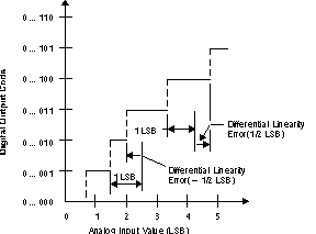
| EDNL | Differential nonlinearity error | Difference between the actual step width and the ideal value. See Figure 6-19. | ±1.5 | LSB | |||
| EINL | Integral nonlinearity error | Maximum deviation from the best straight line through the MibADC. MibADC transfer characteristics, excluding the quantization error. See Figure 6-20. | ±2 | LSB | |||
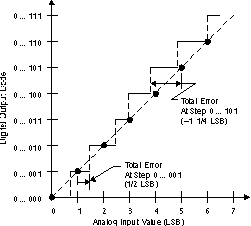
| E TOT | Total error/Absolute accuracy | Maximum value of the difference between an analog value and the ideal midstep value. See Figure 6-21. | ±2.5 | LSB | |||
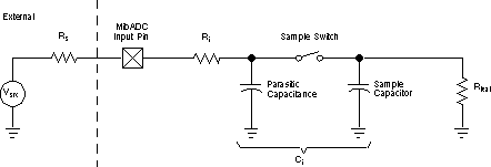 Figure 6-18 MibADC Input Equivalent Circuit
Table 6-21 Multi-Buffer ADC Timing Requirements(1)
| MIN | NOM | MAX | UNIT | ||
|---|---|---|---|---|---|
| tc(ADCLK) | Cycle time, MibADC clock | 0.067 | µs | ||
| td(SH) | Delay time, sample and hold time | 1 | µs | ||
| td(c) | Delay time, conversion time | 0.55 | µs | ||
| td(SHC)(2) | Delay time, total sample/hold and conversion time | 1.55 | µs | ||
The differential nonlinearity error shown in Figure 6-19 (sometimes referred to as differential linearity) is the difference between an actual step width and the ideal value of 1 LSB.
The integral nonlinearity error shown in Figure 6-20 (sometimes referred to as linearity error) is the deviation of the values on the actual transfer function from a straight line.
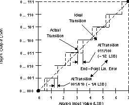
The absolute accuracy or total error of an MibADC as shown in Figure 6-21 is the maximum value of the difference between an analog value and the ideal midstep value.
