SNVS903B December 2012 – May 2016 SM74611
PRODUCTION DATA.
- 1 Features
- 2 Applications
- 3 Description
- 4 Revision History
- 5 Pin Configuration and Functions
- 6 Specifications
- 7 Detailed Description
- 8 Application and Implementation
- 9 Power Supply Recommendations
- 10Layout
- 11Device and Documentation Support
- 12Mechanical, Packaging, and Orderable Information
Package Options
Mechanical Data (Package|Pins)
- KTT|3
Thermal pad, mechanical data (Package|Pins)
Orderable Information
8 Application and Implementation
NOTE
Information in the following applications sections is not part of the TI component specification, and TI does not warrant its accuracy or completeness. TI’s customers are responsible for determining suitability of components for their purposes. Customers should validate and test their design implementation to confirm system functionality.
8.1 Application Information
The SM74611 smart bypass diode is a drop-in replacement for traditional bypass diodes used in photovoltaic (PV) applications. When compared to a typical diode, which has a typical 0.7-V drop during forward conduction, the SM74611 dissipates significantly less power and allows PV applications such as solar junction boxes to run much cooler.
8.2 Typical Application
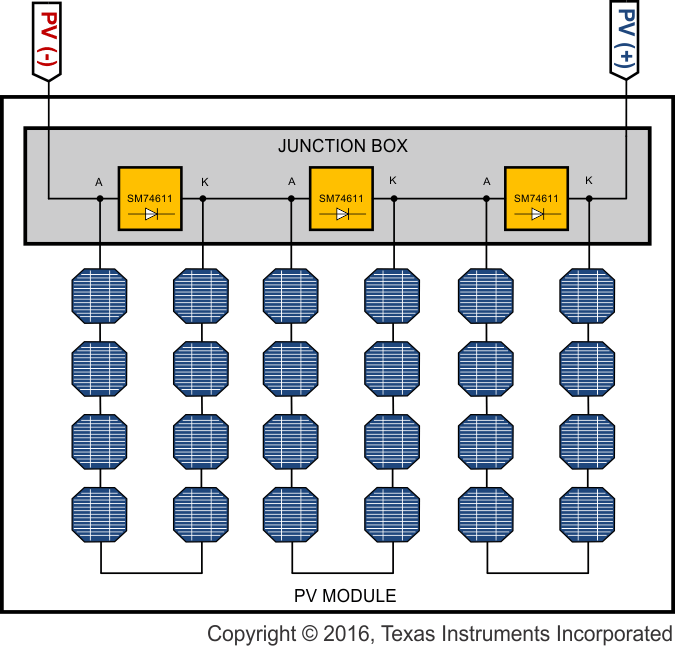
The application diagram shown in Figure 6 shows 3 SM74611 Smart Bypass Diodes connected in series, each providing a bypass path for 8 solar cells for a total of 24 solar cells.
 Figure 6. Solar Junction Box
8.2.1 Design Requirements
Table 1 lists the parameters for Figure 6
Table 1. Design Parameters
| PARAMETER | EXAMPLE VALUE |
|---|---|
| Minimum input voltage VINMIN | 1 V |
| Maximum input voltage VINMAX | 28 V |
| Maximum forward current IMAX | 20 A |
| Junction temperature range TJ | –40°C to 125°C |
8.2.2 Detailed Design Procedure
The SM74611 is primarily used in solar junction boxes to improve the efficiency compared to commonly used P-N junction or Schottky diodes. The junction boxes have 2 or 3 diodes in series connected across the solar panel, each diode connected across a substring of solar cells, as shown in Figure 6. Standard bodies like IEC and UL mandate certain thermal tests for bypass diodes in junction boxes. At the time of this writing, the applicable specifications include IEC61215, IEC61646, EN 50548, IEC62790, and UL3730. The test procedures across these specifications are similar and include the following:
- Apply temperature probe to the diode (in the case of SM74611 the smart bypass diode) body
- Apply 75 ± 50°C to the junction box, containing the 2 to 3 (smart bypass) diodes
- Apply panel-rated, short-circuit current through the box for 1 hour
- Increase the current to 1.25 times the rated value and continue testing for another 1 hour
While the specifications may not specify how the temperature must be maintained, it is expected that there will be no air flow as in a real application behind a solar panel. Also there may be no specification of how the temperature is raised from room to 750°C. TI recommends a gradual and controlled increase to avoid shock to the product under test. Using a good climate chamber or oven is needed to ensure uniformity and consistency of temperature during test and from test of one junction box to another. Similar precautions are also necessary with the thermocouples and temperature probes used during the tests. It is a good idea to check the equipment used with the certification body. The junction box should be operational after these tests. Due to body diode pulses, a simple diode tester cannot be used to test the Smart Bypass Diode. An example testing scheme is shown in Application Curve. To avoid component failure, the Smart Bypass Diode junction temperature must not exceed the maximum rating during these tests. See Absolute Maximum Ratings for the SM74611 limits. The junction temperature is calculated based on the measured values from the temperature probe.
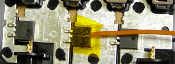
The temperature probe could be applied on the top (plastic case) or bottom (tab) of the SM74611 body, as shown in Figure 7. Methods of applying this probe vary from Kapton tape, 2K-resins (for top) to soldering (bottom tab). It is good to check with the certification body regarding the acceptable method.
 Figure 7. Temperature Probe Attachment During Thermal Test
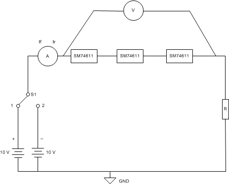
Because the SM74611 Smart Bypass Diode cycles the FET ON and OFF to recharge the charge pump, occasionally the body diode conducts instead of the FET. Therefore the drop across the Smart Bypass Diode is not constant even at constant load. Due to this switching behavior, a normal diode tester can not be used to test the operation of the Smart Bypass Diode. The following test scheme is provided, as an example, with junction box application consideration. See Figure 8 while reading the following test steps:
 Figure 8. Example Test Setup for SM74611
Step 1: Testing Forward voltage drop (set R such that If => 1 A)
- Toggle S1 to position 1
- Make sure to see If reading of 10V/R
- Measure Voltage across 3 SM74611 or 1 ea SM74611
- If the setup is working properly, Vf will be less than 150 mV (Rdson losses)
Potential Fault Conditions
- SM74611 FET is not turning ON -> the measured voltage will be > 500 mV
- SM74611 device is not soldered and open -> No If current is seen
Step 2: Testing Reverse voltage turn OFF
- Toggle S1 to position 2
- Measure current Ir which is expected to be < 1 µA
Potential Fault Conditions
- SM74611 FET is shorted or board short is present, the measured current Ir is same as If but with reverse polarity. (This is only in the case of testing each SM74611 and not applicable for testing 3 together).
8.2.3 Application Curve
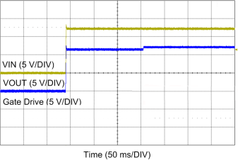
 Figure 9. Start-Up Related to Input Voltage from the Panel