SCDS411D July 2019 – October 2022 SN3257-Q1
PRODUCTION DATA
- 1 Features
- 2 Applications
- 3 Description
- 4 Revision History
- 5 Pin Configuration and Functions
- 6 Specifications
-
7 Parameter Measurement Information
- 7.1 On-Resistance
- 7.2 Off-Leakage Current
- 7.3 On-Leakage Current
- 7.4 IPOFF Leakage Current
- 7.5 Transition Time
- 7.6 tON (EN) and tOFF (EN) Time
- 7.7 tON (VDD) and tOFF (VDD) Time
- 7.8 Break-Before-Make Delay
- 7.9 Propagation Delay
- 7.10 Skew
- 7.11 Charge Injection
- 7.12 Capacitance
- 7.13 Off Isolation
- 7.14 Channel-to-Channel Crosstalk
- 7.15 Bandwidth
- 8 Detailed Description
- 9 Application and Implementation
- 10Power Supply Recommendations
- 11Layout
- 12Device and Documentation Support
- 13Mechanical, Packaging, and Orderable Information
Package Options
Mechanical Data (Package|Pins)
Thermal pad, mechanical data (Package|Pins)
Orderable Information
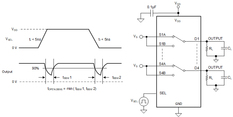
7.8 Break-Before-Make Delay
Break-before-make delay is a safety feature that prevents two inputs from connecting when the device is switching. The output first breaks from the on-state switch before making the connection with the next on-state switch. The time delay between the break and the make is known as break-before-make delay. Figure 7-8 shows the setup used to measure break-before-make delay, denoted by the symbol tOPEN(BBM).
 Figure 7-8 Break-Before-Make Delay Measurement Setup