SCAS541G October 1995 – March 2024 SN54AC574 , SN74AC574
PRODUCTION DATA
- 1
- 1 Features
- 2 Description
- 3 Pin Configuration and Functions
-
4 Specifications
- 4.1 Absolute Maximum Ratings
- 4.2 Recommended Operating Conditions
- 4.3 Thermal Information
- 4.4 Electrical Characteristics
- 4.5 Timing Requirements, VCC = 3.3 V ± 0.3 V
- 4.6 Timing Requirements, VCC = 5 V ± 0.5 V
- 4.7 Switching Characteristics, VCC = 3.3 V ± 0.3 V
- 4.8 Switching Characteristics, VCC = 5 V ± 0.5 V
- 4.9 Operating Characteristics
- 5 Parameter Measurement Information
- 6 Detailed Description
- 7 Application and Implementation
- 8 Device and Documentation Support
- 9 Revision History
- 10Mechanical, Packaging, and Orderable Information
Package Options
Refer to the PDF data sheet for device specific package drawings
Mechanical Data (Package|Pins)
- W|20
- J|20
- FK|20
Thermal pad, mechanical data (Package|Pins)
Orderable Information
2 Description
These 8-bit flip-flops feature 3-state outputs designed specifically for driving highly capacitive or relatively low-impedance loads. The devices are particularly suitable for implementing buffer registers, I/O ports, bidirectional bus drivers, and working registers.
Device Information
| PART NUMBER | PACKAGE(1) | PACKAGE SIZE(2) | BODY SIZE(3) |
|---|---|---|---|
| SNx4AC574 | DB (SSOP, 20) | 7.2mm × 7.8mm | 7.2mm × 5.30mm |
| DW (SOIC, 20) | 12.8mm × 10.3mm | 12.80mm × 7.50mm | |
| N (PDIP, 20) | 24.33mm × 9.4mm | 24.33mm × 6.35mm | |
| PW (TSSOP, 20) | 6.5mm × 6.4mm | 6.50mm × 4.40mm |
(1) For more information, see Section 10.
(2) The package size (length × width)
is a nominal value and includes pins, where applicable.
(3) The body size (length × width) is
a nominal value and does not include pins.
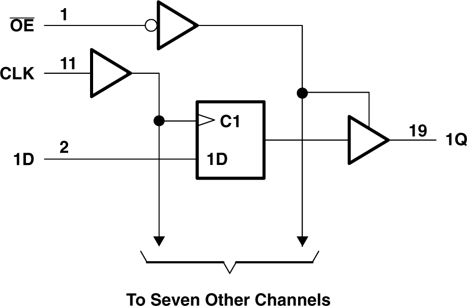
 Logic Diagram (Positive
Logic)