SCAS541G October 1995 – March 2024 SN54AC574 , SN74AC574
PRODUCTION DATA
- 1
- 1 Features
- 2 Description
- 3 Pin Configuration and Functions
-
4 Specifications
- 4.1 Absolute Maximum Ratings
- 4.2 Recommended Operating Conditions
- 4.3 Thermal Information
- 4.4 Electrical Characteristics
- 4.5 Timing Requirements, VCC = 3.3 V ± 0.3 V
- 4.6 Timing Requirements, VCC = 5 V ± 0.5 V
- 4.7 Switching Characteristics, VCC = 3.3 V ± 0.3 V
- 4.8 Switching Characteristics, VCC = 5 V ± 0.5 V
- 4.9 Operating Characteristics
- 5 Parameter Measurement Information
- 6 Detailed Description
- 7 Application and Implementation
- 8 Device and Documentation Support
- 9 Revision History
- 10Mechanical, Packaging, and Orderable Information
Package Options
Refer to the PDF data sheet for device specific package drawings
Mechanical Data (Package|Pins)
- W|20
- J|20
- FK|20
Thermal pad, mechanical data (Package|Pins)
Orderable Information
3 Pin Configuration and Functions
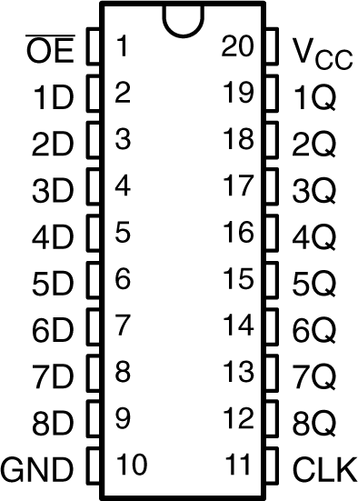
 Figure 3-1 SN54AC574 J or W Package;
SN74AC574 DB, DW, N, NS, or PW Package (Top View)
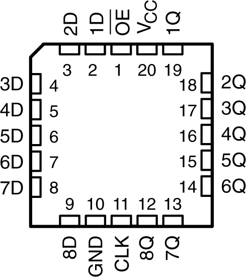
 Figure 3-2 SN54AC574 FK Package (Top
View)
Figure 3-2 SN54AC574 FK Package (Top
View)Table 3-1 Pin Functions
| PIN | I/O | DESCRIPTION | |
|---|---|---|---|
| NAME | NO. | ||
| OE | 1 | Input | Output enable for all channels, active low |
| D1 | 2 | Input | Input for channel 1 |
| D2 | 3 | Input | Input for channel 2 |
| D3 | 4 | Input | Input for channel 3 |
| D4 | 5 | Input | Input for channel 4 |
| D5 | 6 | Input | Input for channel 5 |
| D6 | 7 | Input | Input for channel 6 |
| D7 | 8 | Input | Input for channel 7 |
| D8 | 9 | Input | Input for channel 8 |
| GND | 10 | — | Ground |
| CLK | 11 | Input | Clock input for all channels, rising edge triggered |
| Q8 | 12 | Output | Output for channel 8 |
| Q7 | 13 | Output | Output for channel 7 |
| Q6 | 14 | Output | Output for channel 6 |
| Q5 | 15 | Output | Output for channel 5 |
| Q4 | 16 | Output | Output for channel 4 |
| Q3 | 17 | Output | Output for channel 3 |
| Q2 | 18 | Output | Output for channel 2 |
| Q1 | 19 | Output | Output for channel 1 |
| VCC | 20 | — | Postive supply |
| Thermal Pad | — | The thermal pad can be connect to GND or left floating. Do not connect to any other signal or supply. | |