-
SNx4AC74 Dual Positive-Edge-Triggered D-type Flip-Flops with Clear and Preset
- 1
- 1 Features
- 2 Description
- 3 Pin Configuration and Functions
-
4 Specifications
- 4.1 Absolute Maximum Ratings
- 4.2 Recommended Operating Conditions
- 4.3 Thermal Information
- 4.4 Electrical Characteristics
- 4.5 Timing Requirements, VCC = 3.3 V ± 0.3 V
- 4.6 Timing Requirements, VCC = 5 V ± 0.5 V
- 4.7 Switching Characteristics, VCC = 3.3 V ± 0.3 V
- 4.8 Switching Characteristics, VCC = 5 V ± 0.5 V
- 4.9 Operating Characteristics
- 5 Parameter Measurement Information
- 6 Detailed Description
- 7 Application and Implementation
- 8 Device and Documentation Support
- 9 Revision History
- 10Mechanical, Packaging, and Orderable Information
- IMPORTANT NOTICE
Package Options
Refer to the PDF data sheet for device specific package drawings
Mechanical Data (Package|Pins)
- W|14
Thermal pad, mechanical data (Package|Pins)
Orderable Information
SNx4AC74 Dual Positive-Edge-Triggered D-type Flip-Flops with Clear and Preset
1 Features
- 2V to 6V VCC operation
- Inputs accept voltages to 6V
- Max tpd of 10 ns at 5V
2 Description
The ’AC74 devices are dual positive-edge-triggered D-type flip-flops.
Device
Information
| PART NUMBER | PACKAGE(1) | PACKAGE SIZE (2) | BODY SIZE(3) |
|---|---|---|---|
| SNx4AC74 | PW (TSSOP, 14) | 5 mm × 6.4 mm | 5 mm × 4.40 mm |
| D (SOIC, 14) | 8.65 mm × 6 mm | 8.65 mm × 3.9 mm | |
| DB (SSOP, 14) | 6.2 mm × 7.8 mm | 6.2 mm × 5.3 mm | |
| N (PDIP, 14) | 19.3 mm × 9.4 mm | 19.3 mm × 6.35 mm | |
| NS (SOP, 14) | 10.2 mm × 7.8 mm | 10.3 mm × 5.3 mm |
(1) For more information, see Section
10.
(2) The package size (length × width) is a
nominal value and includes pins, where applicable.
(3) The body size (length × width) is a
nominal value and does not include pins.
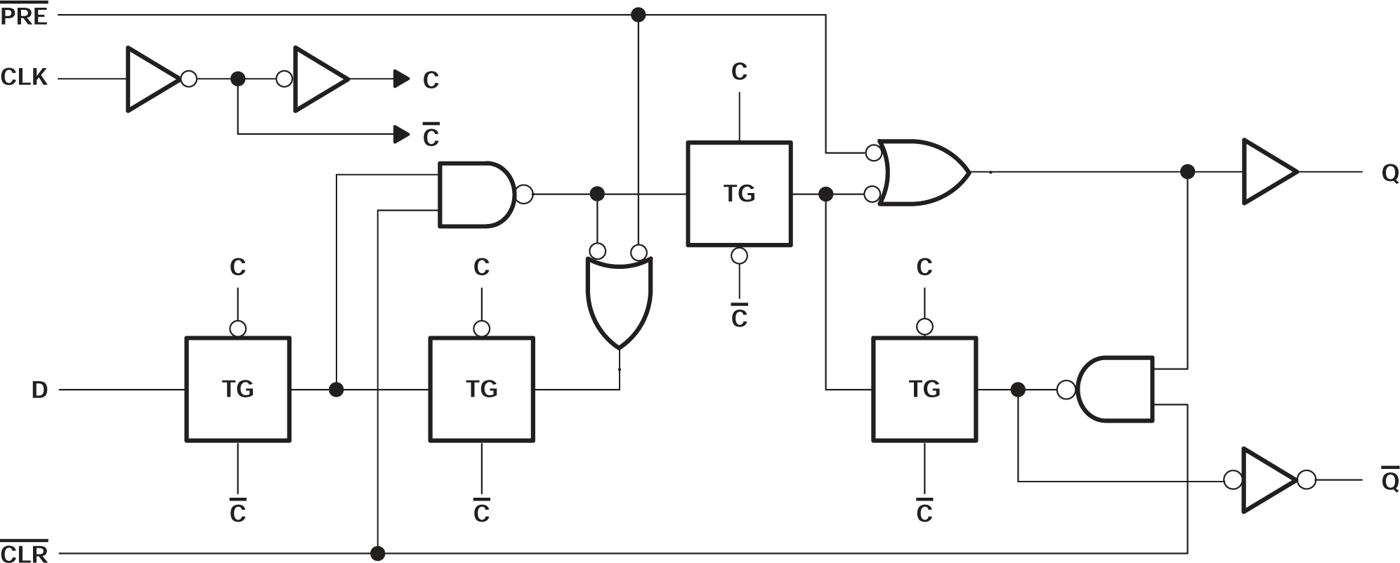
 Logic
Diagram, Each Flip-flop (Positive Logic)
Logic
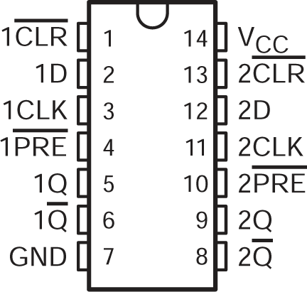
Diagram, Each Flip-flop (Positive Logic)3 Pin Configuration and Functions
 Figure 3-1 SN54AC74 J or W Package; SN74AC74 D, DB, N, NS, or PW Package (Top
View)
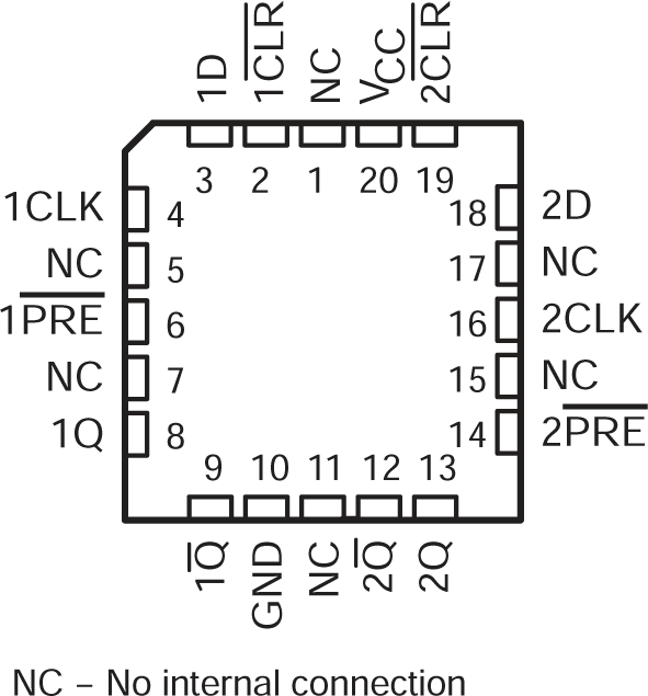
 Figure 3-2 SN54AC74 FK Package (Top View)
| PIN | TYPE(1) | DESCRIPTION | |
|---|---|---|---|
| NAME | NO. | ||
| 1 CLR | 1 | Input | Channel 1, Clear Input, Active Low |
| 1D | 2 | Input | Channel 1, Data Input |
| 1CLK | 3 | Input | Channel 1, Positive edge triggered clock input |
| 1 PRE | 4 | Input | Channel 1, Preset Input, Active Low |
| 1Q | 5 | Output | Channel 1, Output |
| 1 Q | 6 | Output | Channel 1, Inverted Output |
| GND | 7 | — | Ground |
| 2 Q | 8 | Output | Channel 2, Inverted Output |
| 2Q | 9 | Output | Channel 2, Output |
| 2 PRE | 10 | Input | Channel 2, Preset Input, Active Low |
| 2CLK | 11 | Input | Channel 2, Positive edge triggered clock input |
| 2D | 12 | Input | Channel 2, Data Input |
| 2 CLR | 13 | Input | Channel 2, Clear Input, Active Low |
| VCC | 14 | — | Positive Supply |
(1) Signal Types: I = Input, O =
Output, I/O = Input or Output