SCAS531D August 1995 – July 2024 SN54ACT11 , SN74ACT11
PRODUCTION DATA
- 1
- 1 Features
- 2 Description
- 3 Pin Configuration and Functions
- 4 Specifications
- 5 Parameter Measurement Information
- 6 Detailed Description
- 7 Application and Implementation
- 8 Device and Documentation Support
- 9 Revision History
- 10Mechanical, Packaging, and Orderable Information
Package Options
Refer to the PDF data sheet for device specific package drawings
Mechanical Data (Package|Pins)
- FK|20
- W|14
Thermal pad, mechanical data (Package|Pins)
Orderable Information
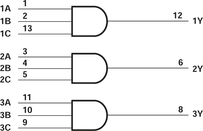
6.1 Functional Block Diagram
 Figure 6-1 Logic Diagram, Each Gate (Positive Logic)
Pin numbers shown are for the D, DB, J, N, NS, PW, and W packages.