SCAS515G June 1995 – March 2024 SN54ACT240 , SN74ACT240
PRODMIX
- 1
- 1 Features
- 2 Applications
- 3 Description
- 4 Pin Configuration and Functions
- 5 Specifications
- 6 Parameter Measurement Information
- 7 Detailed Description
- 8 Device and Documentation Support
- 9 Revision History
- 10Mechanical, Packaging, and Orderable Information
Package Options
Refer to the PDF data sheet for device specific package drawings
Mechanical Data (Package|Pins)
- W|20
- J|20
- FK|20
Thermal pad, mechanical data (Package|Pins)
Orderable Information
3 Description
These octal buffers and line drivers are designed specifically to improve the performance and density of 3-state memory address drivers, clock drivers, and bus-oriented receivers and transmitters.
Package Information
| PART NUMBER | PACKAGE(1) | PACKAGE SIZE(2) | BODY SIZE(3) |
|---|---|---|---|
| SN74ACT240 | N (PDIP, 20) | 24.33mm × 9.4mm | 24.33mm × 6.35mm |
| DGS (VSSOP, 20) | 5.1mm × 4.9mm | 5.1mm × 3mm | |
| DW (SOIC, 20) | 12.8mm × 10.3mm | 12.80mm × 7.50mm | |
| NS (SOP, 20) | 12.6mm × 7.8mm | 12.6mm × 5.3mm | |
| DB (SSOP, 20) | 7.2mm × 7.8mm | 7.2mm × 5.3mm | |
| PW (TSSOP, 20) | 6.5mm × 6.4mm | 6.5mm × 4.4mm | |
| RKS (VQFN, 20) | 4.5mm × 2.5mm | 4.5mm × 2.5mm |
(1) For more information, see Section 10.
(2) The package size (length × width) is a nominal value and includes
pins, where applicable.
(3) The body size (length × width) is
a nominal value and does not include pins.

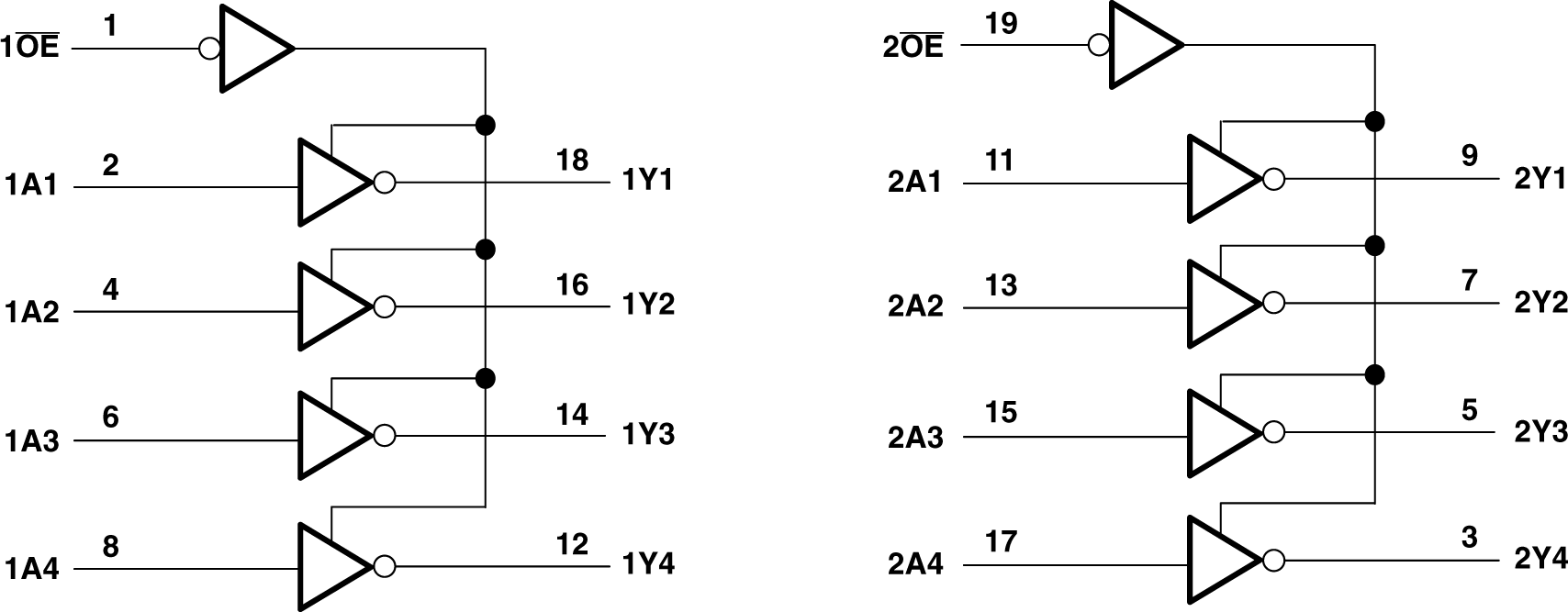
Logic Diagram (Positive Logic)