SCAS520I August 1995 – July 2024 SN54ACT74 , SN74ACT74
PRODUCTION DATA
- 1
- 1 Features
- 2 Description
- 3 Pin Configuration and Functions
- 4 Specifications
- 5 Parameter Measurement Information
- 6 Detailed Description
- 7 Application and Implementation
- 8 Device and Documentation Support
- 9 Revision History
- 10Mechanical, Packaging, and Orderable Information
Package Options
Refer to the PDF data sheet for device specific package drawings
Mechanical Data (Package|Pins)
- J|14
- FK|20
- W|14
Thermal pad, mechanical data (Package|Pins)
Orderable Information
2 Description
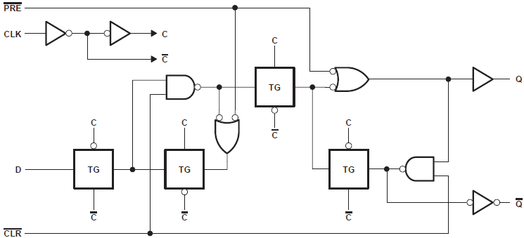
The 'ACT74 dual positive-edge-triggered devices are D-type flip-flops.
Device Information
| PART NUMBER | PACKAGE(1) | PACKAGE SIZE (2) | BODY SIZE(3) |
|---|---|---|---|
| SNx4ACT74 | PW (TSSOP, 14) | 5mm × 6.4mm | 5mm × 4.40mm |
| D (SOIC, 14) | 8.65mm × 6mm | 8.65mm × 3.9mm | |
| DB (SSOP, 14) | 6.2mm × 7.8mm | 6.2mm × 5.3mm | |
| N (PDIP, 14) | 19.3mm × 9.4mm | 19.3mm × 6.35mm | |
| NS (SOP, 14) | 10.2mm × 7.8mm | 10.3mm × 5.3mm |
(1) For more information, see Mechanical, Packaging, and Orderable
Information.
(2) The package size (length × width)
is a nominal value and includes pins, where applicable.
(3) The body size (length × width) is
a nominal value and does not include pins.
 Logic Diagram (Positive Logic)