SCLS258N December 1995 – July 2024 SN54AHC138 , SN74AHC138
PRODUCTION DATA
- 1
- 1 Features
- 2 Description
- 3 Pin Configuration and Functions
- 4 Specifications
- 5 Parameter Measurement Information
- 6 Detailed Description
- 7 Application and Implementation
- 8 Device and Documentation Support
- 9 Revision History
- 10Mechanical, Packaging, and Orderable Information
Package Options
Refer to the PDF data sheet for device specific package drawings
Mechanical Data (Package|Pins)
- W|16
- J|16
- FK|20
Thermal pad, mechanical data (Package|Pins)
Orderable Information
3 Pin Configuration and Functions
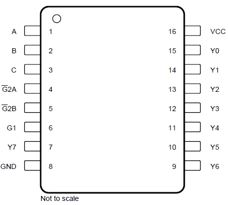
 Figure 3-1 D, DB, DGV , N, NS , or PW Package,
16-Pin SOIC, SSOP, TVSOP, PDIP, SOP, or TSSOP
Figure 3-1 D, DB, DGV , N, NS , or PW Package,
16-Pin SOIC, SSOP, TVSOP, PDIP, SOP, or TSSOP(Top View)
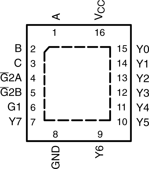
 Figure 3-2 RGY Package,
16-Pin VQFN
(Top View)

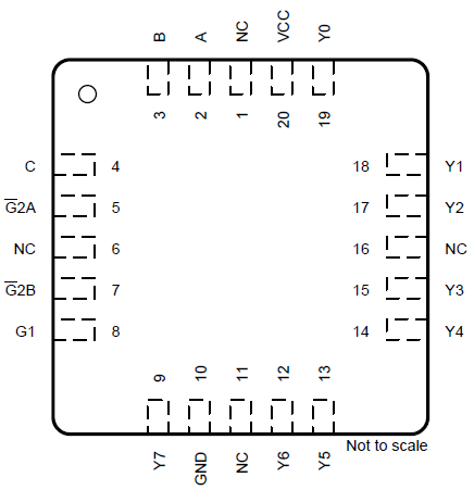
NC: No internal
connection
Figure 3-3 FK
Package,20-Pin LCCC
(Top View)
Table 3-1 Pin Functions
| PIN | TYPE(1) | DESCRIPTION | |
|---|---|---|---|
| NAME | NO. | ||
| A0 | 1 | I | Address select 0 |
| A1 | 2 | I | Address select 1 |
| A2 | 3 | I | Address select 2 |
| G0 | 4 | I | Output strobe 0, active low |
| G1 | 5 | I | Output strobe 1, active low |
| G2 | 6 | I | Output strobe 2 |
| Y7 | 7 | O | Output 7 |
| GND | 8 | G | Ground |
| Y6 | 9 | O | Output 6 |
| Y5 | 10 | O | Output 5 |
| Y4 | 11 | O | Output 4 |
| Y3 | 12 | O | Output 3 |
| Y2 | 13 | O | Output 2 |
| Y1 | 14 | O | Output 1 |
| Y0 | 15 | O | Output 0 |
| VCC | 16 | P | Positive supply |
| Thermal pad(2) | The thermal pad can be connected to GND or left floating. Do not connect to any other signal or supply. | ||
(1) Signal Types: I = Input, O = Output, I/O
= Input or Output, P = Power, G = Ground.
(2) WBQB package only.