SCLS345L May 1996 – July 2024 SN54AHC157 , SN74AHC157
PRODUCTION DATA
- 1
- 1 Features
- 2 Description
- 3 Pin Configuration and Functions
-
4 Specifications
- 4.1 Absolute Maximum Ratings
- 4.2 ESD Ratings
- 4.3 Recommended Operating Conditions
- 4.4 Thermal Information
- 4.5 Electrical Characteristics
- 4.6 Switching Characteristics, VCC = 3.3V ± 0.3V
- 4.7 Switching Characteristics, VCC = 5V ± 0.5V
- 4.8 Noise Characteristics
- 4.9 Operating Characteristics
- 4.10 Typical Characteristics
- 5 Parameter Measurement Information
- 6 Detailed Description
- 7 Application and Implementation
- 8 Device and Documentation Support
- 9 Revision History
- 10Mechanical, Packaging, and Orderable Information
Package Options
Refer to the PDF data sheet for device specific package drawings
Mechanical Data (Package|Pins)
- W|16
- J|16
- FK|20
Thermal pad, mechanical data (Package|Pins)
Orderable Information
2 Description
These quadruple 2-line to 1-line data selectors/multiplexers are designed for 2V to 5.5V VCC operation.
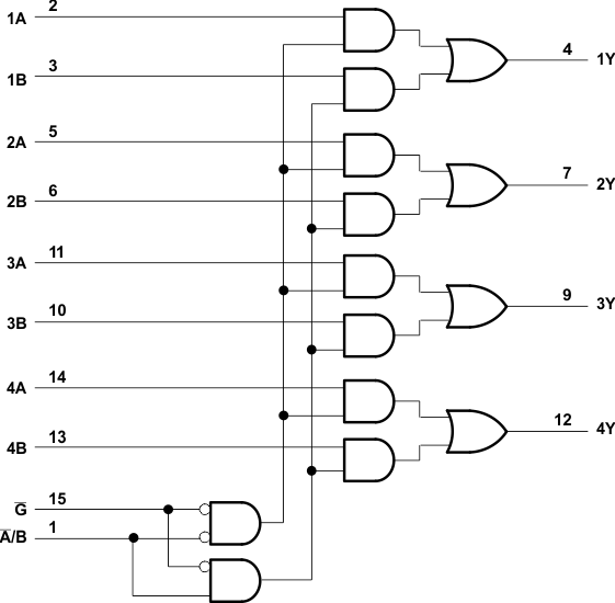
The SNx4AHC157 devices feature a common strobe (G) input. When the strobe is high, all outputs are low. When the strobe is low, a 4-bit word is selected from one of two sources and is routed to the four outputs. The devices provide true data.
Device
Information
| PART NUMBER | PACKAGE(1) | PACKAGE SIZE(2) | BODY SIZE(3) |
|---|---|---|---|
| SNx4AHC157 | D (SOIC, 16) | 9.90mm × 6mm | 9.90mm × 3.90mm |
| DB (SSOP, 16) | 6.20mm × 7.8mm | 6.20mm × 5.30mm | |
| N (PDIP, 16) | 19.31mm × 9.4mm | 19.31mm × 6.35mm | |
| NS (SOP, 16) | 5mm × 6.4mm | 5mm × 4.4mm | |
| PW (TSSOP, 16) | 5.00mm × 6.4mm | 5.00mm × 4.40mm | |
| DGV (TVSOP, 16) | 3.6mm × 6.4mm | 3.6mm × 4.4mm | |
| RGY (VQFN, 16) | 4mm × 3.5mm | 4mm × 3.5mm |
(1) For more information, see Section 10.
(2) The package size (length × width) is a nominal value and includes pins, where
applicable.
(3) The body size (length × width) is a nominal value and does not include pins.

Pin numbers shown are for
the D, DB, DGV, J, N, NS, PW, RGY, and W packages.
Logic
Diagram (Positive Logic)