SCLS345L May 1996 – July 2024 SN54AHC157 , SN74AHC157
PRODUCTION DATA
- 1
- 1 Features
- 2 Description
- 3 Pin Configuration and Functions
-
4 Specifications
- 4.1 Absolute Maximum Ratings
- 4.2 ESD Ratings
- 4.3 Recommended Operating Conditions
- 4.4 Thermal Information
- 4.5 Electrical Characteristics
- 4.6 Switching Characteristics, VCC = 3.3V ± 0.3V
- 4.7 Switching Characteristics, VCC = 5V ± 0.5V
- 4.8 Noise Characteristics
- 4.9 Operating Characteristics
- 4.10 Typical Characteristics
- 5 Parameter Measurement Information
- 6 Detailed Description
- 7 Application and Implementation
- 8 Device and Documentation Support
- 9 Revision History
- 10Mechanical, Packaging, and Orderable Information
Package Options
Refer to the PDF data sheet for device specific package drawings
Mechanical Data (Package|Pins)
- W|16
- J|16
- FK|20
Thermal pad, mechanical data (Package|Pins)
Orderable Information
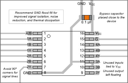
7.2.2 Layout Example
 Figure 7-1 Example
Layout for the SNx4AHC157