SCLS252O October 1995 – July 2024 SN54AHCT240 , SN74AHCT240
PRODUCTION DATA
- 1
- 1 Features
- 2 Applications
- 3 Description
- 4 Pin Configuration and Functions
- 5 Specifications
- Parameter Measurement Information
- 6 Detailed Description
- 7 Application and Implementation
- 8 Device and Documentation Support
- 9 Revision History
- 10Mechanical, Packaging, and Orderable Information
Package Options
Refer to the PDF data sheet for device specific package drawings
Mechanical Data (Package|Pins)
- W|20
- J|20
- FK|20
Thermal pad, mechanical data (Package|Pins)
Orderable Information
Abstract
Unless otherwise noted, all input pulses are supplied by generators having the following characteristics:
- PRR ≤ 1 MHz
- ZO = 50 Ω
- tr ≤ 3 ns
- tf ≤ 3 ns
Note:
All parameters and waveforms are not applicable to all devices.
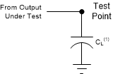
A. CL includes probe and jig capacitance.
B. The outputs are measured one at a time, with one transition per measurement.
Figure 6-1 Load Circuit For Totem-Pole Outputs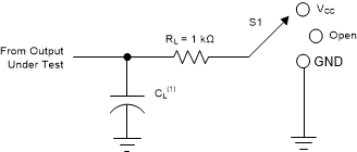
A. CL includes probe and jig capacitance.
B. The outputs are measured one at a time, with one transition per measurement.
Figure 6-2 Load Circuit For Tri-State And Open-Drain OutputsTable 6-1 Loading Conditions For Parameter
| TEST | S1 |
|---|---|
| tPLH(1), tPHL(1) | Open |
| tPLZ(3), tPZL (2) | VCC |
| tPHZ(3), tPZH(2) | GND |
| Open drain | VCC |
(1) tPLH and tPHL are the same as tpd.
(2) tPZL and tPZH are the same as ten.
(3) tPLZ and tPHZ are the same as tdis.
 Figure 6-3 Voltage Waveforms Pulse Durations
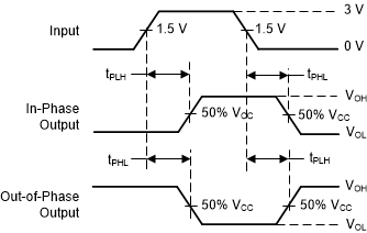
A. The outputs are measured one at a time, with one transition per measurement.
Figure 6-4 Voltage Waveforms Propagation Delay Times Inverting and Noninverting Outputs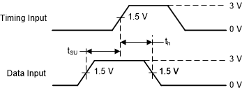 Figure 6-5 Voltage Waveforms Setup And Hold Times
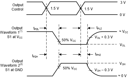
A. Waveform 1 is for an output with internal conditions such that the output is low, except when disabled by the output control.
B. Waveform 2 is for an output with internal conditions such that the output is high, except when disabled by the output control.
C. The outputs are measured one at a time, with one transition per measurement.
Figure 6-6 Voltage Waveforms Enable And Disable Times
Low- and High-Level Enabling