SCBS019D September 1988 – February 2021 SN74BCT374
PRODUCTION DATA
- 1 Features
- 2 Applications
- 3 Description
- 4 Revision History
- 5 Pin Configuration and Functions
- 6 Specifications
- 7 Parameter Measurement Information
- 8 Detailed Description
- 9 Application and Implementation
- 10Power Supply Recommendations
- 11Layout
- 12Device and Documentation Support
- 13Mechanical, Packaging, and Orderable Information
Package Options
Refer to the PDF data sheet for device specific package drawings
Mechanical Data (Package|Pins)
- W|20
- J|20
- FK|20
Thermal pad, mechanical data (Package|Pins)
Orderable Information
5 Pin Configuration and Functions
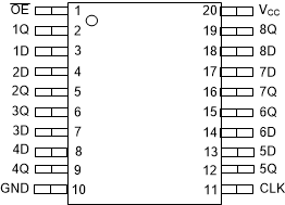
 Figure 5-1 DB, DW, N, NS, J, or W
Package
Figure 5-1 DB, DW, N, NS, J, or W
Package20-Pin SSOP, SOIC, PDIP, SO, CDIP, or CFP
Top View
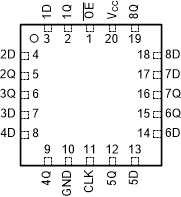
 Figure 5-2 FK Package
20-Pin LCCC
Transparent Top View
Table 5-1 Pin Functions
| PIN | I/O(1) | DESCRIPTION | |
|---|---|---|---|
| NAME | NO. | ||
| OE | 1 | I | Output enable, active low |
| 1Q | 2 | O | Channel 1 output |
| 1D | 3 | I | Channel 1 input |
| 2D | 4 | I | Channel 2 input |
| 2Q | 5 | O | Channel 2 output |
| 3Q | 6 | O | Channel 3 output |
| 3D | 7 | I | Channel 3 input |
| 4D | 8 | I | Channel 4 input |
| 4Q | 9 | O | Channel 4 output |
| GND | 10 | G | Ground |
| CLK | 11 | I | Clock, rising edge triggered |
| 5Q | 12 | O | Channel 5 output |
| 5D | 13 | I | Channel 5 input |
| 6D | 14 | I | Channel 6 input |
| 6Q | 15 | O | Channel 6 output |
| 7Q | 16 | O | Channel 7 output |
| 7D | 17 | I | Channel 7 input |
| 8D | 18 | I | Channel 8 input |
| 8Q | 19 | O | Channel 8 output |
| VCC | 20 | P | Positive supply |
(1) I = Input, O = Output, I/O = Input or Output, G =
Ground, P = Power.