SCAS294Q January 1993 – December 2024 SN54LVC257A , SN74LVC257A
PRODUCTION DATA
- 1
- 1 Features
- 2 Applications
- 3 Description
- 4 Pin Configuration and Functions
- 5 Specifications
- 6 Parameter Measurement Information
- 7 Detailed Description
- Application and Implementation
- 8 Device and Documentation Support
- 9 Revision History
- 10Mechanical, Packaging, and Orderable Information
Package Options
Mechanical Data (Package|Pins)
- W|16
Thermal pad, mechanical data (Package|Pins)
Orderable Information
3 Description
These quadruple 2-line to 1-line data
selectors and multiplexers are designed for 1.65V to 3.6V VCC
operation.
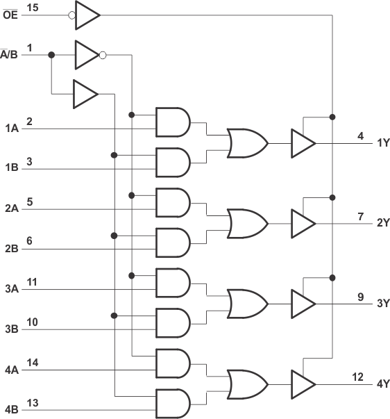
The SNx4LVC257A devices are designed to multiplex signals from 4-bit data sources to 4-output data lines in bus-organized systems. The 3-state outputs do not load the data lines when the output-enable ( OE) input is at a high logic level.
Inputs can be driven from either 3.3V
or 5V devices. This feature allows the use of these devices as translators in a
mixed 3.3V or 5V system
environment.
Device Information
| PART NUMBER | PACKAGE(1) | PACKAGE SIZE(2) | BODY SIZE(3) |
|---|---|---|---|
| SNx4LVC257A | BQB (WQFN, 16) | 3.5mm × 2.5mm | 3.5mm × 2.5mm |
| D (SOIC, 16) | 9.90 mm × 6mm | 9.90 mm × 3.90 mm | |
| DB (SSOP, 16) | 6.20 mm × 7.8mm | 6.20 mm × 5.30 mm | |
| NS (SOP, 16) | 5mm × 6.4mm | 5mm × 4.4mm | |
| PW (TSSOP, 16) | 5.00 mm × 6.4mm | 5.00 mm × 4.40 mm | |
| RGY (VQFN, 16) | 4mm × 3.5mm | 4mm × 3.5mm |
(1) For more information, see Mechanical, Packaging, and Orderable Information.
(2) The package size (length × width)
is a nominal value and includes pins, where applicable.
(3) The body size (length × width) is
a nominal value and does not include pins.

Pin
numbers shown are for the D, DB, J, NS, PW , RGY , and W packages.
Logic Diagram (Positive Logic)