SCAS287V January 1993 – May 2024 SN54LVC74A , SN74LVC74A
PRODUCTION DATA
- 1
- 1 Features
- 2 Applications
- 3 Description
- 4 Pin Configuration and Functions
-
5 Specifications
- 5.1 Absolute Maximum Ratings
- 5.2 ESD Ratings
- 5.3 Recommended Operating Conditions
- 5.4 Thermal Information: SN74LVC74A
- 5.5 Electrical Characteristics
- 5.6 Timing Requirements: SN54LVC74A
- 5.7 Timing Requirements: SN74LVC74A
- 5.8 Timing Requirements: SN74LVC74A, –40°C to 125°C and –40°C to 85°C
- 5.9 Switching Characteristics: SN54LVC74A
- 5.10 Switching Characteristics: SN74LVC74A
- 5.11 Switching Characteristics: SN74LVC74A, –40°C to 125°C and –40°C to 85°C
- 5.12 Operating Characteristics
- 5.13 Typical Characteristics
- 6 Parameter Measurement Information
- 7 Detailed Description
- 8 Application and Implementation
- 9 Device and Documentation Support
- 10Revision History
- 11Mechanical, Packaging, and Orderable Information
Package Options
Refer to the PDF data sheet for device specific package drawings
Mechanical Data (Package|Pins)
- W|14
Thermal pad, mechanical data (Package|Pins)
Orderable Information
3 Description
The SNx4LVC74A devices integrate two positive-edge triggered D-type flip-flops in one convenient device.
The SN54LVC74A is designed for 2.7V to 3.6V VCC operation, and the SN74LVC74A is designed for 1.65V to 3.6V VCC operation.
Device Information
| PART NUMBER | PACKAGE (1) | PACKAGE SIZE(2) | BODY SIZE(3) |
|---|---|---|---|
| SNx4LVC74A | BQA (WQFN, 14) | 3mm × 2.5mm | 3mm × 2.5mm |
| D (SOIC, 14) | 8.65mm x 6mm | 8.65mm × 3.91mm | |
| DB (SSOP, 14) | 6.2mm x 7.8mm | 6.20mm × 5.30mm | |
| NS (SOP, 14) | 10.2mm x 7.8mm | 10.20mm × 5.30mm | |
| PW (TSSOP, 14) | 5mm x 6.4mm | 5.00mm × 4.40mm | |
| RGY (VQFN, 14) | 3.50mm × 3.50mm | 3.50mm × 3.50mm | |
| J (CDIP, 14) | 19.55mm x 7.9mm | 19.56 mm × 6.67 mm | |
| W (CFP, 14) | 9.21mm x 9 mm | 9.21 mm × 5.97 mm | |
| FK (LCCC, 20) | 8.9mm x 8.9mm | 8.89 mm × 8.89 mm |
(1) For more information, see Mechanical, Packaging, and Orderable Information.
(2) The package size (length × width)
is a nominal value and includes pins, where applicable.
(3) The body size (length × width) is
a nominal value and does not include pins.
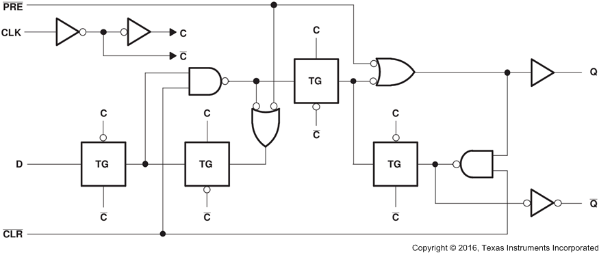
 Logic Diagram, Each Flip-Flop (Positive
Logic)