SDLS025D December 1983 – May 2017 SN5400 , SN54LS00 , SN54S00 , SN7400 , SN74LS00 , SN74S00
PRODUCTION DATA.
- 1 Features
- 2 Applications
- 3 Description
- 4 Revision History
- 5 Pin Configuration and Functions
-
6 Specifications
- 6.1 Absolute Maximum Ratings
- 6.2 ESD Ratings: SN74LS00
- 6.3 Recommended Operating Conditions
- 6.4 Thermal Information
- 6.5 Electrical Characteristics: SNx400
- 6.6 Electrical Characteristics: SNx4LS00
- 6.7 Electrical Characteristics: SNx4S00
- 6.8 Switching Characteristics: SNx400
- 6.9 Switching Characteristics: SNx4LS00
- 6.10 Switching Characteristics: SNx4S00
- 6.11 Typical Characteristics
- 7 Parameter Measurement Information
- 8 Detailed Description
- 9 Application and Implementation
- 10Power Supply Recommendations
- 11Layout
- 12Device and Documentation Support
- 13Mechanical, Packaging, and Orderable Information
Package Options
Refer to the PDF data sheet for device specific package drawings
Mechanical Data (Package|Pins)
- J|14
- FK|20
- W|14
Thermal pad, mechanical data (Package|Pins)
Orderable Information
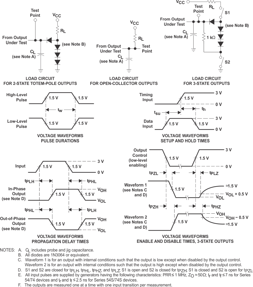
7 Parameter Measurement Information
7.1 Propagation Delays, Setup and Hold Times, and Pulse Width
 Figure 2. Load Circuits and Voltage Waveforms