SCES952 august 2023 SN54SC245-SEP
PRODUCTION DATA
- 1
- 1 Features
- 2 Applications
- 3 Description
- 4 Revision History
- 5 Pin Configuration and Functions
-
6 Specifications
- 6.1 Absolute Maximum Ratings
- 6.2 ESD Ratings
- 6.3 Recommended Operating Conditions
- 6.4 Thermal Information
- 6.5 Electrical Characteristics
- 6.6 Switching Characteristics 1.2-V VCC
- 6.7 Switching Characteristics 1.8-V VCC
- 6.8 Switching Characteristics 2.5-V VCC
- 6.9 Switching Characteristics 3.3-V VCC
- 6.10 Switching Characteristics 5-V VCC
- 6.11 Noise Characteristics
- 6.12 Typical Characteristics
- 7 Parameter Measurement Information
- 8 Detailed Description
- 9 Application and Implementation
- 10Device and Documentation Support
- 11Mechanical, Packaging, and Orderable Information
Package Options
Mechanical Data (Package|Pins)
- PW|20
Thermal pad, mechanical data (Package|Pins)
Orderable Information
3 Description
SN54SC245-SEP is an octal bus
transceiver with 3-state outputs. All eight channels
are controlled by the direction (DIR) pin and
output enable (OE) pin. The
output enable (OE) controls
all outputs in the device. When the
OE pin is in the low state,
the appropriate outputs as determined by the
direction (DIR) pin are enabled. When the
OE pin is in the high state,
all outputs of the device are disabled. All
disabled outputs are placed into the
high-impedance state.
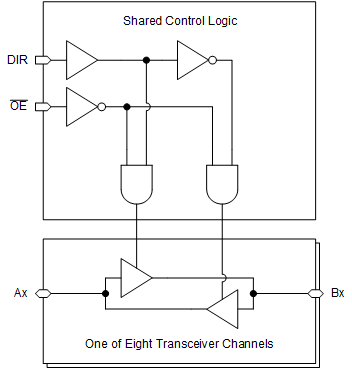
 Simplified Logic
Diagram
Package
Information
| PART NUMBER | PACKAGE(1) | PACKAGE SIZE(2) | BODY SIZE (NOM)(3) |
|---|---|---|---|
| SN54SC245-SEP | PW (TSSOP, 20) | 6.5 mm × 6.4 mm | 6.5 mm × 4.4 mm |
(1) For all available packages,
see the orderable addendum at the end of the data
sheet.
(2) The package size (length ×
width) is a nominal value and includes pins, where
applicable.
(3) The body size (length ×
width) is a nominal value and does not include
pins.
 Simplified Logic
Diagram