SCLS959 November 2023 SN54SC2T74-SEP
PRODUCTION DATA
- 1
- 1 Features
- 2 Applications
- 3 Description
- 4 Pin Configuration and Functions
- 5 Specifications
- 6 Parameter Measurement Information
- 7 Detailed Description
- 8 Application and Implementation
- 9 Device and Documentation Support
- 10Revisiqon History
- 11Mechanical, Packaging, and Orderable Information
Package Options
Refer to the PDF data sheet for device specific package drawings
Mechanical Data (Package|Pins)
- PW|14
Thermal pad, mechanical data (Package|Pins)
Orderable Information
3 Description
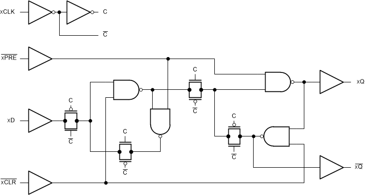
The SN54SC2T74-SEP contains two independent D-type positive-edge-triggered flip-flops. A low level at the preset (PRE) input sets the output high. A low level at the clear (CLR) input resets the output low. Preset and clear functions are asynchronous and not dependent on the levels of the other inputs. When PRE and CLR are inactive (high), data at the data (D) input meeting the setup time requirements is transferred to the outputs (Q, Q) on the positive-going edge of the clock (CLK) pulse. Clock triggering occurs at a voltage level and is not directly related to the rise time of the input clock (CLK) signal. Following the hold-time interval, data at the data (D) input can be changed without affecting the levels at the outputs (Q, Q). The output level is referenced to the supply voltage (VCC) and supports 1.8-V, 2.5-V, 3.3-V, and 5-V CMOS levels.
The input is designed with a lower threshold circuit to support up translation for lower voltage CMOS inputs (for example, 1.2 V input to 1.8 V output or 1.8 V input to 3.3 V output). In addition, the 5-V tolerant input pins enable down translation (for example, 3.3 V to 2.5 V output).
| PART NUMBER | PACKAGE(1) | PACKAGE SIZE(2) | BODY SIZE (NOM)(3) |
|---|---|---|---|
| SN54SC2T74-SEP | PW (TSSOP, 14) | 5.00 mm × 6.40 mm | 5.00 mm × 4.40 mm |
 Simplified Logic Diagram