SCAS991 April 2024 SN54SC8T541-SEP
ADVANCE INFORMATION
- 1
- 1 Features
- 2 Applications
- 3 Description
- 4 Pin Configuration and Functions
- 5 Specifications
- 6 Parameter Measurement Information
- 7 Detailed Description
- 8 Application and Implementation
- 9 Device and Documentation Support
- 10Revision History
- 11Mechanical, Packaging, and Orderable Information
Package Options
Refer to the PDF data sheet for device specific package drawings
Mechanical Data (Package|Pins)
- PW|20
Thermal pad, mechanical data (Package|Pins)
Orderable Information
3 Description
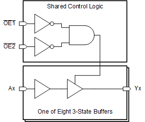
The SN54SC8T541-SEP contains eight buffers with 3-state outputs. The active low output enable pins (OE1 and OE2) control all eight channels, and are configured so that both must be low for the outputs to be active. When the outputs are enabled, the outputs are actively driven low or high. When the outputs are disabled, the outputs are set into the high-impedance state. The output level is referenced to the supply voltage (VCC) and supports 1.8V, 2.5V, 3.3V, and 5V CMOS levels.
The input is designed with a lower threshold circuit to support up translation for lower voltage CMOS inputs (for example, 1.2V input to 1.8V output or 1.8V input to 3.3V output). In addition, the 5V tolerant input pins enable down translation (for example, 3.3V to 2.5V output).
| PART NUMBER | PACKAGE(1) | PACKAGE SIZE(2) | BODY SIZE (NOM)(3) |
|---|---|---|---|
| SN54SC8T541-SEP | PW (TSSOP, 20) | 6.5 mm × 6.4 mm | 6.5 mm × 4.4 mm |
 Simplified Logic Diagram (Positive Logic)