SCAS992 March 2024 SN54SC8T595-SEP
ADVANCE INFORMATION
- 1
- 1 Features
- 2 Applications
- 3 Description
- 4 Pin Configuration and Functions
- 5 Specifications
- 6 Parameter Measurement Information
- 7 Detailed Description
- 8 Application and Implementation
- 9 Device and Documentation Support
- 10Revision History
- 11Mechanical, Packaging, and Orderable Information
Package Options
Mechanical Data (Package|Pins)
- PW|16
Thermal pad, mechanical data (Package|Pins)
Orderable Information
3 Description
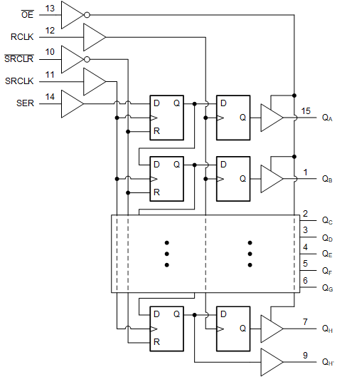
The SN54SC8T595-SEP device contains an 8-bit, serial-in, parallel-out shift register that feeds an 8-bit D-type storage register. The storage register has parallel 3-state outputs. Separate clocks are provided for both the shift and storage register. The shift register has a direct overriding clear ( SRCLR) input, serial (SER) input, and a serial output (QH') for cascading. When the output-enable ( OE) input is high, the outputs are in a high-impedance state. Internal register data is not impacted by the operation of the OE input. The output level is referenced to the supply voltage (VCC) and supports 1.8V, 2.5V, 3.3V, and 5V CMOS levels.
The input is designed with a lower threshold circuit to support up translation for lower voltage CMOS inputs (for example, 1.2V input to 1.8V output or 1.8V input to 3.3V output). In addition, the 5V tolerant input pins enable down translation (for example, 3.3V to 2.5V output).
| PART NUMBER | PACKAGE(1) | PACKAGE SIZE(2) | BODY SIZE (NOM)(3) |
|---|---|---|---|
| SN54SC8T595-SEP | PW (TSSOP, 16) | 5mm × 6.4mm | 5mm × 4.4mm |
 Simplified Logic Diagram (Positive Logic)