SLLSF98 December   2018 SN55HVD233-SEP

PRODUCTION DATA.  

  1. Features
  2. Applications
  3. Description
    1.     Device Images
      1.      Simplified Schematic
  4. Revision History
  5. Description (continued)
  6. Pin Configuration and Functions
    1.     Pin Functions
  7. Specifications
    1. 7.1  Absolute Maximum Ratings
    2. 7.2  ESD Ratings
    3. 7.3  Recommended Operating Conditions
    4. 7.4  Thermal Information
    5. 7.5  Driver Electrical Characteristics
    6. 7.6  Receiver Electrical Characteristics
    7. 7.7  Driver Switching Characteristics
    8. 7.8  Receiver Switching Characteristics
    9. 7.9  Device Switching Characteristics
    10. 7.10 Typical Characteristics
  8. Parameter Measurement Information
  9. Detailed Description
    1. 9.1 Overview
    2. 9.2 Functional Block Diagram
    3. 9.3 Feature Description
      1. 9.3.1 Modes
      2. 9.3.2 Loopback
      3. 9.3.3 CAN Bus States
      4. 9.3.4 ISO 11898 Compliance of SN55HVD233-SEP
        1. 9.3.4.1 Introduction
        2. 9.3.4.2 Differential Signal
          1. 9.3.4.2.1 Common-Mode Signal
        3. 9.3.4.3 Interoperability of 3.3-V CAN in 5-V CAN Systems
      5. 9.3.5 Thermal Shutdown
    4. 9.4 Device Functional Modes
  10. 10Application and Implementation
    1. 10.1 Application Information
      1. 10.1.1 Diagnostic Loopback
    2. 10.2 Typical Application
      1. 10.2.1 Design Requirements
      2. 10.2.2 Detailed Design Procedure
        1. 10.2.2.1 Slope Control
        2. 10.2.2.2 Standby
      3. 10.2.3 Application Curves
  11. 11Power Supply Recommendations
  12. 12Layout
    1. 12.1 Layout Guidelines
      1. 12.1.1 Bus Loading, Length, and Number of Nodes
      2. 12.1.2 CAN Termination
    2. 12.2 Layout Example
  13. 13Device and Documentation Support
    1. 13.1 Receiving Notification of Documentation Updates
    2. 13.2 Community Resources
    3. 13.3 Trademarks
    4. 13.4 Electrostatic Discharge Caution
    5. 13.5 Glossary
  14. 14Mechanical, Packaging, and Orderable Information

Package Options

Mechanical Data (Package|Pins)
Thermal pad, mechanical data (Package|Pins)
Orderable Information

Typical Characteristics

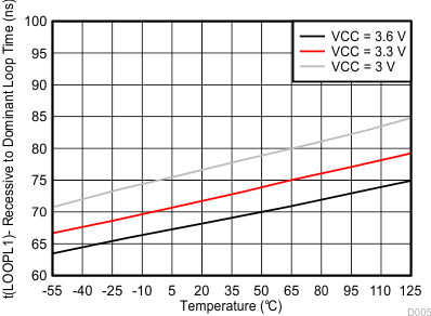
SN55HVD233-SEP D005-sllsei2.gif
V(RS), V(LBK) = 0 V
Figure 1. Recessive-To-Dominant Loop Time vs
Temperature
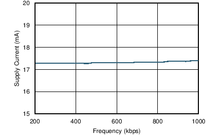
SN55HVD233-SEP C003_SLLSIE2.png
VCC = 3.3 V V(RS), V(LBK) = 0 V TA = 25°C
60-Ω load
Figure 3. Supply Current vs Frequency
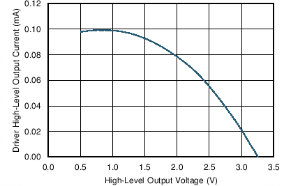
SN55HVD233-SEP C005_SLLSIE2.png
VCC = 3.3 V V(RS), V(LBK) = 0 V TA = 25°C
Figure 5. Driver High-Level Output Current vs
High-Level Output Voltage
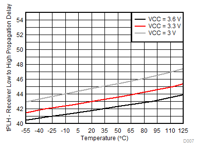
SN55HVD233-SEP D007-sllsei2.gif
V(RS), V(LBK) = 0 V See Figure 17
Figure 7. Receiver Low-To-High Propagation Delay vs
Temperature
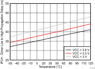
SN55HVD233-SEP D004-sllsei2.gif
V(RS), V(LBK) = 0 V See Figure 15
Figure 9. Driver Low-To-High Propagation Delay vs
Temperature
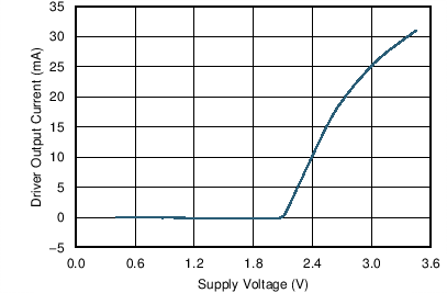
SN55HVD233-SEP C011_SLLSIE2.png
V(RS), V(LBK) = 0 V TA = 25°C RL = 60 Ω
Figure 11. Driver Output Current vs Supply Voltage
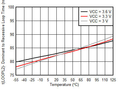
SN55HVD233-SEP D002-sllsei2.gif
V(RS), V(LBK) = 0 V
Figure 2. Dominant-To-Recessive Loop Time vs
Temperature
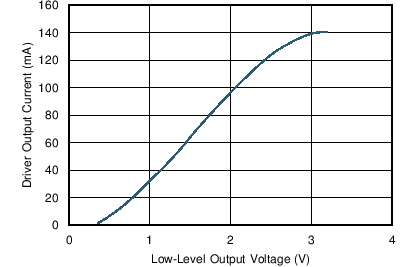
SN55HVD233-SEP C004_SLLSIE2.png
VCC = 3.3 V V(RS), V(LBK) = 0 V TA = 25°C
Figure 4. Driver Low-Level Output Current vs
Low-Level Output Voltage
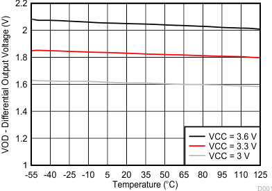
SN55HVD233-SEP D001-sllsei2.gif
RL = 60 Ω V(RS), V(LBK) = 0 V
Figure 6. Differential Output Voltage vs
Temperature
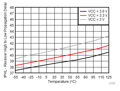
SN55HVD233-SEP D006-sllsei2.gif
V(RS), V(LBK) = 0 V See Figure 17
Figure 8. Receiver High-To-Low Propagation Delay vs
Temperature
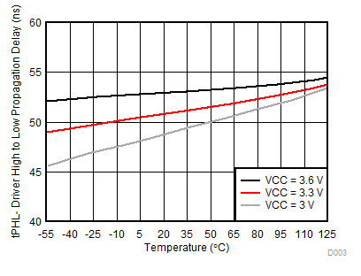
SN55HVD233-SEP D003-sllsei2.gif
V(RS), V(LBK) = 0 V See Figure 15
Figure 10. Driver High-To-Low Propagation Delay vs
Temperature