SLLS545G November 2002 – October 2015 SN55HVD251 , SN65HVD251
PRODUCTION DATA.
- 1 Features
- 2 Applications
- 3 Description
- 4 Revision History
- 5 Pin Configuration and Functions
-
6 Specifications
- 6.1 Absolute Maximum Ratings
- 6.2 ESD Ratings
- 6.3 Recommended Operating Conditions
- 6.4 Thermal Information
- 6.5 Supply Current
- 6.6 Electrical Characteristics: Driver
- 6.7 Electrical Characteristics: Receiver
- 6.8 VREF-Pin Characteristics
- 6.9 Power Dissipation Characteristics
- 6.10 Switching Characteristics: Driver
- 6.11 Switching Characteristics: Device
- 6.12 Switching Characteristics: Receiver
- 6.13 Dissipation Ratings
- 6.14 Typical Characteristics
- 7 Parameter Measurement Information
- 8 Detailed Description
- 9 Application and Implementation
- 10Power Supply Recommendations
- 11Layout
- 12Device and Documentation Support
- 13Mechanical, Packaging, and Orderable Information
Package Options
Mechanical Data (Package|Pins)
- DRJ|8
Thermal pad, mechanical data (Package|Pins)
- DRJ|8
Orderable Information
6 Specifications
6.1 Absolute Maximum Ratings(1)(2)
| MIN | MAX | UNIT | |||
|---|---|---|---|---|---|
| Supply voltage, VCC | –0.3 | 7 | V | ||
| Voltage at any bus pin(CANH or CANL) | –36 | 36 | V | ||
| Transient voltage per ISO 7637, pulse 1, 2, 3a, 3b | CANH, CANL | –200 | 200 | V | |
| Input voltage, VI (D, Rs, or R) | –0.3 | VCC + 0.5 | V | ||
| Receiver output current, IO | –10 | 10 mA | mA | ||
| Electrical fast transient/burst | IEC 61000-4-4, Classification B | CANH, CANL | –3 | 3 | kV |
| Continuous total power dissipation | (see Dissipation Ratings) | ||||
(1) Stresses beyond those listed under Absolute Maximum Ratings may cause permanent damage to the device. These are stress ratings only and functional operation of the device at these or any other conditions beyond those indicated under Recommended Operating Conditions is not implied. Exposure to absolute-maximum-rated conditions for extended periods may affect device reliability.
(2) All voltage values, except differential I/O bus voltages, are with respect to network ground pin.
6.2 ESD Ratings
| VALUE | UNIT | ||||
|---|---|---|---|---|---|
| V(ESD) | Electrostatic discharge | Human body model (HBM), per ANSI/ESDA/JEDEC JS-001(1) | All pins | ±6000 | V |
| CANH, CANL and GND | ±14000 | ||||
| Charged-device model (CDM), per JEDEC specification JESD22-C101(2) | ±1000 | ||||
(1) JEDEC document JEP155 states that 500-V HBM allows safe manufacturing with a standard ESD control process.
(2) JEDEC document JEP157 states that 250-V CDM allows safe manufacturing with a standard ESD control process.
6.3 Recommended Operating Conditions
| MIN | NOM | MAX | UNIT | ||||
|---|---|---|---|---|---|---|---|
| Supply voltage, VCC | 4.5 | 5.5 | V | ||||
| Voltage at any bus terminal (separately or common mode) VI or VIC | –7(1) | 12 | V | ||||
| High-level input voltage, VIH | D input | 0.7 VCC | V | ||||
| Low-level input voltage, VIL | D input | 0.3 VCC | V | ||||
| Differential input voltage, VID | –6 | 6 | V | ||||
| Input voltage to Rs, VI(Rs) | 0 | VCC | V | ||||
| Input voltage at Rs for standby, VI(Rs) | 0.75 VCC | VCC | V | ||||
| Rs wave-shaping resistance | 0 | 100 | kΩ | ||||
| High-level output current, IOH | Driver | –50 | mA | ||||
| Receiver | –4 | ||||||
| Low-level output current, IOL | Driver | 50 | mA | ||||
| Receiver | 4 | ||||||
| Operating free-air temperature, TA | SN65HVD251 | –40 | 125 | °C | |||
| SN55HVD251 | –55 | 125 | |||||
| Junction temperature, TJ | 145 | °C | |||||
(1) The algebraic convention, in which the least positive (most negative) limit is designated as minimum is used in this data sheet.
6.4 Thermal Information
| THERMAL METRIC(1) | SN55HVD251 | SN65HVD251 | UNIT | ||
|---|---|---|---|---|---|
| DRJ (SON) | D (SOIC) | P (PDIP) | |||
| 8 PINS | 8 PINS | 8 PINS | |||
| RθJC(top) | Junction-to-case (top) thermal resistance | 52 | 44.6 | 66.6 | °C/W |
| RθJB | Junction-to-board thermal resistance | 73 | 78.7 | 48.9 | °C/W |
(1) For more information about traditional and new thermal metrics, see the Semiconductor and IC Package Thermal Metrics application report, SPRA953.
6.5 Supply Current
over operating free-air temperature range (unless otherwise noted)| PARAMETER | TEST CONDITIONS | MIN | TYP(1) | MAX | UNIT | |||
|---|---|---|---|---|---|---|---|---|
| ICC | Supply current | Standby | Rs at VCC, D at VCC | 275 | µA | |||
| Dominant | D at 0 V, 60-Ω load, Rs at 0 V | 65 | mA | |||||
| Recessive | D at VCC, no load, Rs at 0 V | 14 | ||||||
(1) All typical values are at 25°C and with a 5-V supply.
6.6 Electrical Characteristics: Driver
over recommended operating conditions (unless otherwise noted).| PARAMETER | TEST CONDITIONS | MIN | TYP(1) | MAX | UNIT | |||
|---|---|---|---|---|---|---|---|---|
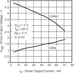
| VO(D) | Bus output voltage (Dominant) | CANH | Figure 10 and Figure 11 , D at 0 V Rs at 0 V, T ≥ –40°C |
2.75 | 3.5 | 4.5 | V | |
| CANL | 0.5 | 2 | ||||||
| VO(R) | Bus output voltage (Recessive) | CANH | Figure 10 and Figure 11 , D at 0.7 VCC, Rs at 0 V |
2 | 2.5 | 3 | ||
| CANL | 2 | 2.5 | 3 | |||||
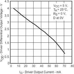
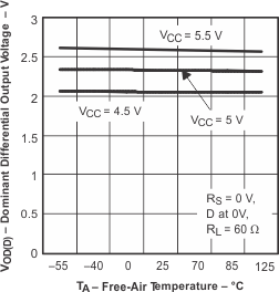
| VOD(D) | Differential output voltage (Dominant) | Figure 10 , D at 0 V, Rs at 0 V | 1.5 | 2 | 3 | V | ||
| Figure 12 , D at 0 V, Rs at 0 V, RNODE = 330 Ω | 1.2 | 2 | 3.1 | V | ||||
| Figure 12 , D at 0 V, Rs at 0 V, RNODE = 165 Ω, VCC ≥ 4.75 V | 1.2 | 2 | 3.1 | V | ||||
| VOD(R) | Differential output voltage (Recessive) | Figure 10 and Figure 11 , D at 0.7 VCC | –120 | 12 | mV | |||
| D at 0.7 VCC, no load, T ≤ 85°C | –0.5 | 0.05 | V | |||||
| VOC(pp) | Peak-to-peak common-mode output voltage | Figure 18, Rs at 0 V | 600 | mV | ||||
| IIH | High-level input current, D Input | D at 0.7 VCC | –40 | 0 | µA | |||
| IIL | Low-level input current, D Input | D at 0.3 VCC | –60 | 0 | µA | |||
| IOS(SS) | Short-circuit steady-state output current | Figure 20, VCANH at –7 V, CANL Open | –200 | mA | ||||
| Figure 20, VCANH at 12 V, CANL Open | 2.5 | |||||||
| Figure 20, VCANL at -7 V, CANH Open | –2 | |||||||
| Figure 20, VCANL at 12 V, CANH Open | 200 | |||||||
| CO | Output capacitance | See receiver input capacitance | ||||||
| IOZ | High-impedance output current | See receiver input current | ||||||
| IIRs(s) | Rs input current for standby | Rs at 0.75 VCC | –10 | µA | ||||
| IIRs(f) | Rs input current for full speed operation | Rs at 0 V | –550 | 0 | µA | |||
(1) All typical values are at 25°C and with a 5-V supply.
6.7 Electrical Characteristics: Receiver
over recommended operating conditions (unless otherwise noted).| PARAMETER | TEST CONDITIONS | MIN | TYP | MAX | UNIT | ||||
|---|---|---|---|---|---|---|---|---|---|
| VIT+ | Positive-going input threshold voltage | Rs at 0 V, (See Table 1) | 750 | 900 | mV | ||||
| VIT- | Negative-going input threshold voltage | 500 | 650 | ||||||
| Vhys | Hysteresis voltage (VIT+ - VIT-) | 100 | |||||||
| VOH | High-level output voltage | Figure 15, IO = –4 mA | 0.8 VCC | V | |||||
| VOL | Low-level output voltage | Figure 15, IO = 4 mA | 0.2 VCC | V | |||||
| II | Bus input current | CANH or CANL at 12 V | Other bus pin at 0 V, Rs at 0 V, D at 0.7 VCC | 600 | µA | ||||
| CANH or CANL at 12 V, VCC at 0 V | 715 | ||||||||
| CANH or CANL at -7 V | –460 | ||||||||
| CANH or CANL at -7 V, VCC at 0 V | –340 | ||||||||
| CI | Input capacitance, (CANH or CANL) | Pin-to-ground, VI = 0.4 sin (4E6πt) + 0.5 V, D at 0.7 VCC | 20 | pF | |||||
| CID | Differential input capacitance | Pin-to-pin, VI = 0.4 sin (4E6πt) + 0.5 V, D at 0.7 VCC | 10 | pF | |||||
| RID | Differential input resistance | D at 0.7 VCC, Rs at 0 V | 40 | 100 | kΩ | ||||
| RIN | Input resistance, (CANH or CANL) | D at 0.7 VCC, Rs at 0 V | 20 | 50 | kΩ | ||||
| Receiver noise rejection | See Figure 22 | ||||||||
6.8 VREF-Pin Characteristics
over recommended operating conditions (unless otherwise noted).| PARAMETER | TEST CONDITIONS | MIN | TYP | MAX | UNIT | |
|---|---|---|---|---|---|---|
| VO | Reference output voltage | –5 µA < IO < 5 µA | 0.45 VCC | 0.55 VCC | V | |
| –50 µA < IO < 50 µA | 0.4 VCC | 0.6 VCC | ||||
6.9 Power Dissipation Characteristics
| PARAMETER | TEST CONDITIONS | MIN | TYP | MAX | UNIT | ||
|---|---|---|---|---|---|---|---|
| PD | Device power dissipation | VCC = 5 V, Tj = 27°C, RL = 60 Ω, RS at 0 V, Input to D a 500-kHz 50% duty cycle square wave |
97.7 | mW | |||
| VCC = 5.5 V, Tj = 130°C, RL = 60 Ω, RS at 0 V, Input to D a 500-kHz 50% duty cycle square wave |
142 | mW | |||||
| TSD | Thermal shutdown junction temperature | 165 | °C | ||||
6.10 Switching Characteristics: Driver
over recommended operating conditions (unless otherwise noted).| PARAMETER | TEST CONDITIONS | MIN | TYP | MAX | UNIT | |
|---|---|---|---|---|---|---|
| tpLH | Propagation delay time, low-to-high-level output | Figure 13, Rs at 0 V | 40 | 70 | ||
| Figure 13, Rs with 10 kΩ to ground | 90 | 125 | ||||
| Figure 13, Rs with 100 kΩ to ground | 500 | 800 | ||||
| tpHL | Propagation delay time, high-to-low-level output | Figure 13, Rs at 0 V | 85 | 125 | ||
| Figure 13, Rs with 10 kΩ to ground | 200 | 260 | ||||
| Figure 13, Rs with 100 kΩ to ground | 1150 | 1450 | ||||
| tsk(p) | Pulse skew (|tpHL - tpLH|) | Figure 13, Rs at 0 V | 45 | 85 | ||
| Figure 13, Rs with 10 kΩ to ground | 110 | 180 | ns | |||
| Figure 13, Rs with 100 kΩ to ground | 650 | 900 | ||||
| tr | Differential output signal rise time | Figure 13, Rs at 0 V | 35 | 80 | 100 | |
| tf | Differential output signal fall time | 35 | 80 | 100 | ||
| tr | Differential output signal rise time | Figure 13, Rs with 10 kΩ to ground | 100 | 150 | 250 | |
| tf | Differential output signal fall time | 100 | 150 | 250 | ||
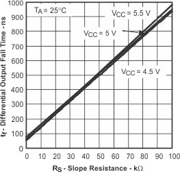
| tr | Differential output signal rise time | Figure 13, Rs with 100 kΩ to ground | 600 | 950 | 1550 | |
| tf | Differential output signal fall time | 600 | 950 | 1550 | ||
| ten | Enable time from standby to dominant | Figure 17 | 0.5 | µs | ||
6.11 Switching Characteristics: Device
over recommended operating conditions (unless otherwise noted).| PARAMETER | TEST CONDITIONS | MIN | TYP | MAX | UNIT | |
|---|---|---|---|---|---|---|
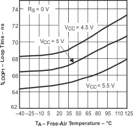
| tloop1 | Total loop delay, driver input to receiver output, recessive to dominant | Figure 19, Rs at 0 V | 60 | 100 | ns | |
| Figure 19, Rs with 10 kΩ to ground | 100 | 150 | ||||
| Figure 19, Rs with 100 kΩ to ground | 440 | 800 | ||||
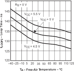
| tloop2 | Total loop delay, driver input to receiver output, dominant to recessive | Figure 19, Rs at 0 V | 115 | 150 | ns | |
| Figure 19, Rs with 10 kΩ to ground | 235 | 290 | ||||
| Figure 19, Rs with 100 kΩ to ground | 1070 | 1450 | ||||
| tloop2 | Total loop delay, driver input to receiver output, dominant to recessive | Figure 19, Rs at 0 V, VCC from 4.5 V to 5.1 V | 105 | 145 | ns | |
6.12 Switching Characteristics: Receiver
over recommended operating conditions (unless otherwise noted).| PARAMETER | TEST CONDITIONS | MIN | TYP | MAX | UNIT | |
|---|---|---|---|---|---|---|
| tpLH | Propagation delay time, low-to-high-level output | Figure 15 | 35 | 50 | ||
| tpHL | Propagation delay time, high-to-low-level output | 35 | 50 | |||
| tsk(p) | Pulse skew (|tpHL - tpLH|) | 20 | ns | |||
| tr | Output signal rise time | 2 | 4 | |||
| tf | Output signal fall time | 2 | 4 | |||
| tp(sb) | Propagation delay time in standby | Figure 21, Rs at VCC | 500 | |||
6.13 Dissipation Ratings
| PACKAGE | CIRCUIT BOARD MODEL | TA = 25°C POWER RATING |
DERATING FACTOR (1) ABOVE TA = 25°C | TA = 85°C POWER RATING | TA = 125°C POWER RATING |
|---|---|---|---|---|---|
| SOIC (D) | Low-K(2) | 576 mW | 4.8 mW/°C | 288 mW | 96 mW |
| High-K(3) | 924 mW | 7.7 mW/°C | 462 mW | 154 mW | |
| PDIP (P) | Low-K(2) | 888 mW | 7.4 mW/°C | 444 mW | 148 mW |
| High-K(3) | 1212 mW | 10.1 mW/°C | 606 mW | 202 mW | |
| WSON (DRJ) | Low-K(2) | 403 mW | 4.03 mW/°C | 262 mW | 100 mW |
| High-K (no Vias)(3) |
1081 mW | 10.8 mW/°C | 703 mW | 270 mW | |
| High-K (with Vias) |
2793 mW | 27.9 mW/°C | 1815 mW | 698 mW |
(1) This is the inverse of the junction-to-ambient thermal resistance when board-mounted and with no air flow.
(2) In accordance with the Low-K thermal metric definitions of EIA/JESD51-3.
(3) In accordance with the High-K thermal metric definitions of EIA/JESD51-7.
6.14 Typical Characteristics
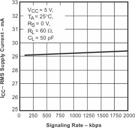 Figure 3. Supply Current (RMS) vs Signaling Rate
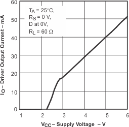 Figure 7. Driver Output Current vs Supply Voltage
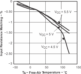 Figure 9. Input Resistance Matching vs Free-Air Temperature
