SLLS101H July 1985 – December 2021 SN65176B , SN75176B
PRODUCTION DATA
- 1 Features
- 2 Applications
- 3 Description
- 4 Revision History
- 5 Pin Configuration and Functions
- 6 Specifications
- 7 Detailed Description
- 8 Application and Implementation
- 9 Power Supply Recommendations
- 10Layout
- 11Device and Documentation Support
- 12Mechanical, Packaging, and Orderable Information
Package Options
Refer to the PDF data sheet for device specific package drawings
Mechanical Data (Package|Pins)
- D|8
- P|8
Thermal pad, mechanical data (Package|Pins)
Orderable Information
6.8 Typical Characteristics
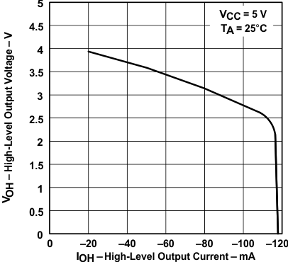 Figure 6-1 Driver High-Level Output Voltage vs High-Level Output Current
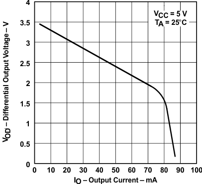 Figure 6-3 Driver Differential Output Voltage vs Output Current
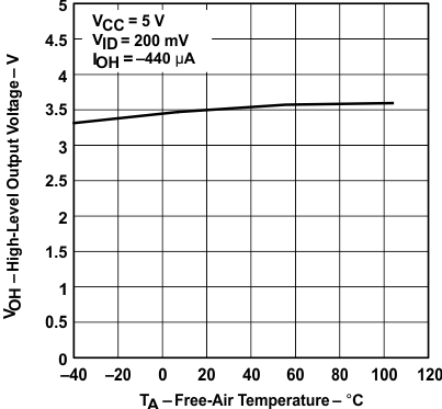
| Only the 0°C to 70°C portion of the curve applies to the SN75176B device. |
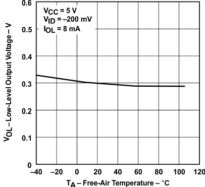 Figure 6-7 Receiver Low-Level Output Voltage vs Free-Air Temperature
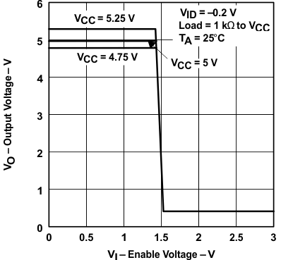 Figure 6-9 Receiver Output Voltage vs Enable Voltage
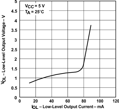 Figure 6-2 Driver Low-Level Output Voltage vs Low-Level Output Current
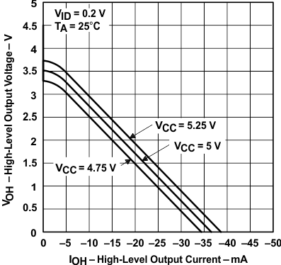 Figure 6-4 Receiver High-Level Output Voltage vs High-Level Output Current
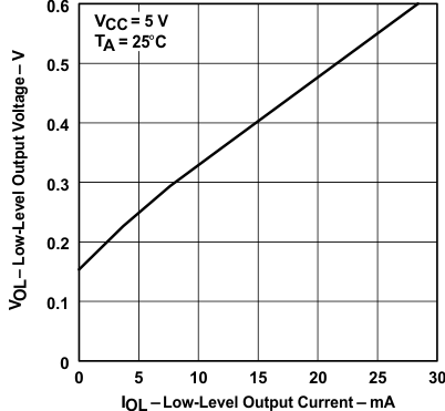
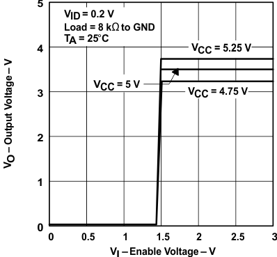 Figure 6-8 Receiver Output Voltage vs Enable Voltage