SLLS052H August 1987 – January 2023 SN65ALS180 , SN75ALS180
PRODUCTION DATA
- 1 Features
- 2 Description
- 3 Revision History
- 4 Pin Configuration and Functions
-
5 Specifications
- 5.1 Absolute Maximum Ratings
- 5.2 Recommended Operating Conditions
- 5.3 Thermal Information
- 5.4 Electrical Characteristics - Driver
- 5.5 Switching Characteristics - Driver
- 5.6 Symbol Equivalents
- 5.7 Electrical Characteristics - Receivers
- 5.8 Switching Characteristics - Receivers
- 5.9 Typical Characteristics
- 6 Parameter Measurement Information
- 7 Detailed Description
- 8 Application and Implementation
- 9 Device and Documentation Support
- 10Mechanical, Packaging, and Orderable Information
Package Options
Refer to the PDF data sheet for device specific package drawings
Mechanical Data (Package|Pins)
- D|14
Thermal pad, mechanical data (Package|Pins)
- D|14
Orderable Information
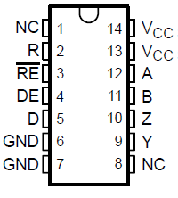
4 Pin Configuration and Functions

NC – No internal connection
Figure 4-1 SN65ALS180 D PackageSN75ALS180 D or N Package
(Top View)
Table 4-1 Pin Functions
| NO | Name | Type | Description |
|---|---|---|---|
| 1 | NC | - | No Internal connection |
| 2 | R | O | Receive data output |
| 3 | RE | I | Receiver enable, active low |
| 4 | DE | I | Driver enable, active high |
| 5 | D | I | Driver data input |
| 6, 7 | GND | GND | Device ground |
| 8 | NC | - | No Internal connection |
| 9 | Y | O | Digital bus output, Y (Complementary to Z) |
| 10 | Z | O | Digital bus output, Z (Complementary to Y) |
| 11 | A | I | Bus input, A (complementary to B) |
| 12 | B | I | Bus input, B (complementary to A) |
| 13, 14 | VCC | SUPPLY | 4.75V to 5.25V supply |