SLLSFC4 July 2019 SN65C1168E-SEP
PRODUCTION DATA.
- 1 Features
- 2 Applications
- 3 Description
- 4 Revision History
- 5 Pin Configuration and Functions
- 6 Specifications
- 7 Parameter Measurement Information
- 8 Detailed Description
- 9 Application and Implementation
- 10Power Supply Recommendations
- 11Device and Documentation Support
- 12Mechanical, Packaging, and Orderable Information
Package Options
Mechanical Data (Package|Pins)
- PW|16
Thermal pad, mechanical data (Package|Pins)
Orderable Information
7 Parameter Measurement Information
 Figure 1. Driver Test Circuit, VOD and VOC
A. C1, C2, and C3 include probe and jig capacitance.
B. The input pulse is supplied by a generator having the following characteristics: PRR = 1 MHz, duty cycle = 50%, tr = tf ≤ 6 ns.
Figure 2. Driver Test Circuit and Voltage Waveforms 
A. C1, C2, and C3 include probe and jig capacitance.
B. The input pulse is supplied by a generator having the following characteristics: PRR = 1 MHz, duty cycle = 50%, tr = tf ≤ 6 ns.
Figure 3. Driver Test Circuit and Voltage Waveforms 
A. C1, C2, and C3 include probe and jig capacitance.
B. The input pulse is supplied by a generator having the following characteristics: PRR = 1 MHz, duty cycle = 50%, tr = tf ≤ 6 ns.
Figure 4. Driver Test Circuit and Voltage Waveforms 
A. C1, C2, and C3 include probe and jig capacitance.
B. The input pulse is supplied by a generator having the following characteristics: PRR = 1 MHz, duty cycle = 50%, tr = tf ≤ 6 ns.
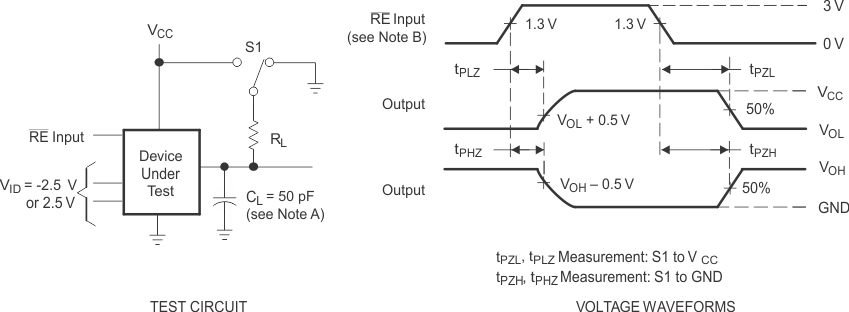
Figure 5. Receiver Test Circuit and Voltage Waveforms 
A. C1, C2, and C3 include probe and jig capacitance.
B. The input pulse is supplied by a generator having the following characteristics: PRR = 1 MHz, duty cycle = 50%, tr = tf ≤ 6 ns.
Figure 6. Receiver Test Circuit and Voltage Waveforms