SLLSEO9D March 2016 – October 2024 SN65DPHY440SS , SN75DPHY440SS
PRODUCTION DATA
- 1
- 1 Features
- 2 Applications
- 3 Description
- 4 Pin Configuration and Functions
- 5 Specifications
-
6 Detailed Description
- 6.1 Overview
- 6.2 Functional Block Diagram
- 6.3 Feature Description
- 6.4 Device Functional Modes
- 6.5
Register Maps
- 6.5.1 BIT Access Tag Conventions
- 6.5.2 Standard CSR Registers (address = 0x000 - 0x07)
- 6.5.3 Standard CSR Register (address = 0x08)
- 6.5.4 Standard CSR Register (address = 0x09)
- 6.5.5 Standard CSR Register (address = 0x0A)
- 6.5.6 Standard CSR Register (address = 0x0B)
- 6.5.7 Standard CSR Register (address = 0x0D)
- 6.5.8 Standard CSR Register (address = 0x0E)
- 6.5.9 Standard CSR Register (address = 0x10) [reset = 0xFF]
- 6.5.10 Standard CSR Register (address = 0x11) [reset = 0xFF]
- 7 Application and Implementation
- 8 Device and Documentation Support
- 9 Revision History
- 10Mechanical, Packaging, and Orderable Information
Package Options
Mechanical Data (Package|Pins)
- RHR|28
Thermal pad, mechanical data (Package|Pins)
- RHR|28
Orderable Information
5.8 Switching Characteristics
over operating free-air temperature range (unless otherwise noted)
| PARAMETER | TEST CONDITIONS | MIN | TYP (1) | MAX | UNIT | |
|---|---|---|---|---|---|---|
| I2C (ERC (SDA), EQ (SCL)) | ||||||
| F(SCL) | I2C Clock Frequency | 100 | kHz | |||
| tF_I2C | Fall time of both SDA and SCL signals | Load of 350 pF with 2-K pullup resistor. Measure at 30% - 70% | 300 | ns | ||
| tR_I2C | Rise Time of both SDA and SCL signals | 1000 | ns | |||
| DPHY LINK | ||||||
| F(BR) | Bit Rate | 1.5 | Gbps | |||
| F(HSCLK) | HS Clock Input range | 100 | 750 | MHz | ||
| F(DESKEW) | Automatic Deskew range | 220 | 750 | MHz | ||
| MIPI DPHY HS Receiver Interface (DA0P/N, DA1P/N, DA2P/N, DA3P/N, DACP/N) | ||||||
| ∆V(CMRX_HF) | Common-mode Interface beyond 450 MHz | 100 | mV | |||
| ∆V(CMRX_LF) | Common-mode interference 50 MHz – 450 MHz | –50 | 50 | mV | ||
| MIPI DPHY HS Transmitter Interface (DB0P/N, DB1P/N, DB2P/N, DB3P/N, DBCP/N) | ||||||
| ∆V(CMRX_HF) | Common-level variations above 450 MHz | 5 | mVrms | |||
| ∆V(CMRX_LF) | Common-level variation between 50 MHz – 450 MHz. | 25 | mVpeak | |||
| tR and tF | 20% - 80% rise time and fall time | Datarate ≤ 1 Gbps | 0.3 | UI | ||
| Datarate > 1 Gbps | 0.35 | UI | ||||
| 100 | ps | |||||
| MIPI DPHY LP Receiver Interface (DA0P/N, DA1P/N, DA2P/N, DA3P/N, DACP/N, DB0P/N) | ||||||
| eSPIKE | Input Pulse rejection | 300 | V ps | |||
| tMIN(RX) | Minimum pulse width response | 20 | ns | |||
| V(INT) | Peak interference amplitude | 200 | mv | |||
| F(INT) | Interference Frequency | 450 | Mhz | |||
| t(LP-PULSE-RX) | Pulse Width of the XOR of DAxP and DAxN | First LP XOR clock pulse after Stop state or last pulse before Stop state. | 42 | ns | ||
| All other pulses. | 22 | ns | ||||
| MIPI DPHY LP Transmitter Interface (DB0P/N, DB1P/N, DB2P/N, DB3P/N, DBCP/N, DA0P/N) | ||||||
| tREOT | 30% - 85% rise time and fall time | Measured at end of HS transmission. | 35 | ns | ||
| t(LP-PULSE-TX) | Pulse Width of the LP XOR clock | First LP XOR clock pulse after Stop state or last pulse before Stop state | 40 | ns | ||
| All other pulses | 20 | ns | ||||
| t(LP-PER-TX) | Period of the LP XOR clock | 90 | ns | |||
| δV/δtsr | Slew Rate at CLOAD = 70 pF | 150 | mV/ns | |||
| Slew Rate at CLOAD = 0 pF Falling edge only | 30 | mV/ns | ||||
| Slew Rate at CLOAD = 0 pF Rising edge only | 30 | mV/ns | ||||
| CLOAD | Load Capacitance | 70 | pF | |||
(1) (1) All typical values are at VCC = 3.3 V, and TA = 25°C.
 Figure 5-1 I2C Timing
 Figure 5-2 DPHY HS RX and TX Timing
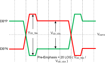
 Figure 5-3 DPHY HS TX
Pre-Emphasis