SLLSEH0F July 2013 – August 2014 SN65HVD01
PRODUCTION DATA.
- 1 Features
- 2 Applications
- 3 Description
- 4 Revision History
- 5 Pin Configuration and Functions
- 6 Specifications
- 7 Parameter Measurement Information
- 8 Detailed Description
- 9 Applications and Implementation
- 10Power Supply Recommendations
- 11Layout
- 12Device and Documentation Support
- 13Mechanical, Packaging, and Orderable Information
Package Options
Mechanical Data (Package|Pins)
- DRC|10
Thermal pad, mechanical data (Package|Pins)
Orderable Information
9 Applications and Implementation
9.1 Application Information
The SN65HVD01 is a half-duplex RS-485 transceiver commonly used for asynchronous data transmissions. The driver and receiver enable terminals allow for the configuration of different operating modes.
 Figure 18. SN65HVD01 Transceiver Configurations
Using independent enable lines provides the most flexible control as it allows for the driver and the receiver to be turned on and off individually. While this configuration requires two control lines, it allows for selective listening into the bus traffic, whether the driver is transmitting data or not.
Combining the enable signals simplifies the interface to the controller by forming a single, direction-control signal. Thus, when the direction- control line is high, the transceiver is configured as a driver, while for a low the device operates as a receiver.
Tying the receiver-enable to ground and controlling only the driver-enable input, also uses one control line only. In this configuration, a node not only receives the data from the bus but also the data it sends and thus can verify that the correct data have been transmitted.
9.2 Typical Application
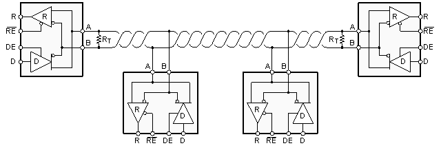
An RS-485 bus consists of multiple transceivers connecting in parallel to a bus cable. To eliminate line reflections, each cable end is terminated with a termination resistor, RT, whose value matches the characteristic impedance, Z0, of the cable. This method, known as parallel termination, allows for higher data rates over longer cable length.
 Figure 19. Typical RS-485 Network with SN65HVD01 Transceivers
9.2.1 Design Requirements
RS-485 is a robust electrical standard suitable for long-distance networking that may be used in a wide range of applications with varying requirements, such as distance, data rate, and number of nodes.
9.2.1.1 Data Rate and Bus Length
The maximum bus length is limited by the transmission line losses and the signal jitter at a given data rate. Because data reliability sharply decreases for a jitter of 10% or more of the baud period, Figure 20 shows the cable length versus data rate characteristic of a conventional RS-485 cable for signal jitter of 10%.
 Figure 20. Cable Length vs Data Rate
9.2.1.2 Bus Loading
The RS-485 standard specifies that a compliant driver must be able to drive 32 unit loads (UL), where 1 unit load represents a load impedance of approximately 12kΩ. Because the SN65HVD01 is a 1/8 UL transceiver, it is possible to connect up to 256 devices to the bus.
9.2.2 Detailed Design Procedure
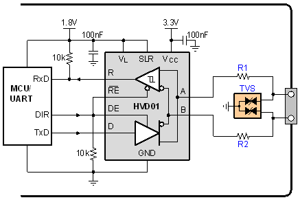
In order to protect bus nodes against high-energy transients, the implementation of external transient protection devices is therefore necessary. Figure 21 suggests a protection circuit against 10 kV ESD, 4 kV EFT, and 1 kV surge transients.
 Figure 21. Transient Protection Against ESD, EFT, and Surge Transients
Table 4. Recommended Materials
| Device | Function | Order Number |
|---|---|---|
| XCVR | 3.3V, 250kbps RS-485 Transceiver | SN65HVD01D |
| R1,R2 | 10Ω, Pulse-Proof Thick-Film Resistor | CRCW0603010RJNEAHP |
| TVS | Bidirectional 400W Transient Suppressor | CDSOT23-SM712 |

