SLLS631E April 2007 – August 2015 SN65HVD1040
PRODUCTION DATA.
- 1 Features
- 2 Applications
- 3 Description
- 4 Revision History
- 5 Description (continued)
- 6 Pin Configuration and Functions
-
7 Specifications
- 7.1 Absolute Maximum Ratings
- 7.2 ESD Ratings
- 7.3 Recommended Operating Conditions
- 7.4 Thermal Information
- 7.5 Driver Electrical Characteristics
- 7.6 Receiver Electrical Characteristics
- 7.7 Device Switching Characteristics
- 7.8 Driver Switching Characteristics
- 7.9 Receiver Switching Characteristics
- 7.10 Dissipation Ratings
- 7.11 Supply Current
- 7.12 Split-Pin Characteristics
- 7.13 STB-Pin Characteristics
- 7.14 Typical Characteristics
- 8 Parameter Measurement Information
- 9 Detailed Description
- 10Application and Implementation
- 11Power Supply Recommendations
- 12Layout
- 13Device and Documentation Support
- 14Mechanical, Packaging, and Orderable Information
Package Options
Mechanical Data (Package|Pins)
- D|8
Thermal pad, mechanical data (Package|Pins)
Orderable Information
9 Detailed Description
9.1 Overview
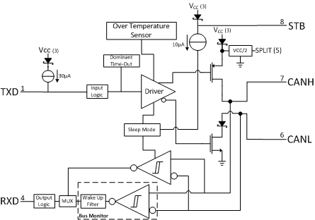
The SN65HVD1040 CAN bus transceiver meets or exceeds the ISO 11898 standard as a high-speed controller area network (CAN) bus physical layer device. The device is designed to interface between the differential bus lines in controller area network and the CAN protocol controller at data rates up to 1 Mbps.
9.2 Functional Block Diagram

9.3 Feature Description
9.3.1 Mode Control
9.3.1.1 High-Speed Mode
Select the high-speed mode of the device operation by setting the STB pin low. The CAN bus driver and receiver are fully operational and the CAN communication is bidirectional. The driver is translating a digital input on TXD to a differential output on CANH and CANL. The receiver is translating the differential signal from CANH and CANL to a digital output on RXD.
9.3.1.2 Low-Power Mode
If a high logic level is applied to the STB pin, the device enters a low-power bus-monitor standby mode. While the SN65HVD1040 is in the low-power bus-monitor standby mode, a dominant bit greater than 5 μs on the bus is passed by the bus-monitor circuit to the receiver output. The local protocol controller may then reactivate the device when it needs to transmit to the bus.
9.3.2 Dominant State Time-Out
During normal mode, the mode where the CAN driver is active, the TXD DTO circuit prevents the transceiver from blocking network communication in the event of a hardware or software failure where TXD is held dominant longer than the time-out period tTXD_DTO. The DTO circuit is triggered on a falling edge on the driver input, TXD. The DTO circuit disables the CAN bus driver if no rising edge is seen on TXD before the time-out period expires. This frees the CAN bus for communication between other nodes on the network. The CAN driver is re-enabled when a rising edge is seen on the drvier input, TXD, thus clearing the TXD DTO condition. The receiver and RXD pin still reflect the CAN bus, and the bus pins are biased to recessive level during a TXD DTO.
NOTE
The minimum dominant TXD time allowed by the TXD DTO circuit limits the minimum possible transmitted data rate on the device. The CAN protocol allows a maximum of eleven successive dominant bits (on TXD) for the worst case, where five successive dominant bits are followed immediately by an error frame. This, along with the tTXD_DTO minimum, limits the minimum data rate. Calculate the minimum transmitted data rate using: Minimum Data Rate = 11 / tTXD_DTO.
9.3.3 Thermal Shutdown
The SN65HVD1040 has a thermal shutdown that turns off the driver outputs when the junction temperature nears 190°C. This shutdown prevents catastrophic failure from bus shorts, but does not protect the circuit from possible damage. The user should strive to maintain recommended operating conditions, and not exceed absolute maximum ratings at all times. If the SN65HVD1040 is subjected to many or long durations faults that can put the device into thermal shutdown, it should be replaced.
9.3.4 SPLIT
A reference voltage (VCC/2) is available through the SPLIT outpit pin. The SPLIT voltage should be tied to the common mode point in a split termination network, hence the pin name, to help stabilize the output common mode voltage. See Figure 29 for more application specific information on properly terminating the CAN bus.
9.3.5 Operating Temperature Range
The SN65HVD1040 is characterized for operation from –40°C to 125°C.
9.4 Device Functional Modes
Table 2. Driver Function Table(1)
| INPUTS | OUTPUTS | BUS STATE | ||
|---|---|---|---|---|
| TXD | STB | CANH | CANL | |
| L | L | H | L | DOMINANT |
| H | L | Z | Z | RECESSIVE |
| Open | X | Z | Z | RECESSIVE |
| X | H or Open | Z | Z | RECESSIVE |
Table 3. Receiver Function Table(1)
| DIFFERENTIAL INPUTS VID = CANH - CANL |
STB | OUTPUT RXD | BUS STATE |
|---|---|---|---|
| VID ≥ 0.9 V | L | L | DOMINANT |
| VID ≥ 1.15 V | H or Open | L | DOMINANT |
| 0.5 V < VID < 0.9 V | X | ? | ? |
| VID ≤ 0.5 V | X | H | RECESSIVE |
| Open | X | H | RECESSIVE |
Table 4. Parametric Cross Reference With the TJA1040
| TJA1040(1) | PARAMETER | HVD10xx |
|---|---|---|
| TJA1040 DRIVER SECTION | ||
| VIH | High-level input voltage | Recommended VIH |
| VIL | Low-level input voltage | Recommended VIL |
| IIH | High-level input current | Driver IIH |
| IIL | Low-level input current | Driver IIL |
| TJA1040 BUS SECTION | ||
| Vth(dif) | Differential input voltage | Receiver VIT and recommended VID |
| Vhys(dif) | Differential input hysteresis | Receiver Vhys |
| VO(dom) | Dominant output voltage | Driver VO(D) |
| VO(reces) | Recessive output voltage | Driver VO(R) |
| VI(dif)(th) | Differential input voltage | Receiver VIT and recommended VID |
| VO(dif0(bus) | Differential bus voltage | Driver VOD(D) and VOD(R) |
| ILI | Power-off bus input current | Receiver II(off) |
| IO(SC) | Short-circuit output current | Driver IOS(SS) |
| RI(cm) | CANH, CANL input resistance | Receiver RIN |
| RI(def) | Differential input resistance | Receiver RID |
| RI(cm) (m) | Input resistance matching | Receiver RI (m) |
| CI(cm) | Input capacitance to ground | Receiver CI |
| CI(dif) | Differential input capacitance | Receiver CID |
| TJA1040 RECEIVER SECTION | ||
| IOH | High-level output current | Recommended IOH |
| IOL | Low-level output current | Recommended IOL |
| TJA1040 SPLIT PIN SECTION | ||
| VO | Reference output voltage | VO |
| TJA1040 TIMING SECTION | ||
| td(TXD-BUSon) | Delay TXD to bus active | Driver tPLH |
| td(TXD-BUSoff) | Delay TXD to bus inactive | Driver tPHL |
| td(BUSon-RXD) | Delay bus active to RXD | Receiver tPHL |
| td(BUSoff-RXD) | Delay bus inactive to RXD | Receiver tPLH |
| tPD(TXD–RXD) | Prop delay TXD to RXD | Device tLOOP1 and tLOOP2 |
| td(stb-norm) | Enable time from standby to dominant | Driver ten |
| TJA1040 STB PIN SECTION | ||
| VIH | High-level input voltage | Recommended VIH |
| VIL | Low-level input voltage | Recommended VIL |
| IIH | High-level input current | IIH |
| IIL | Low-level input current | IIL |
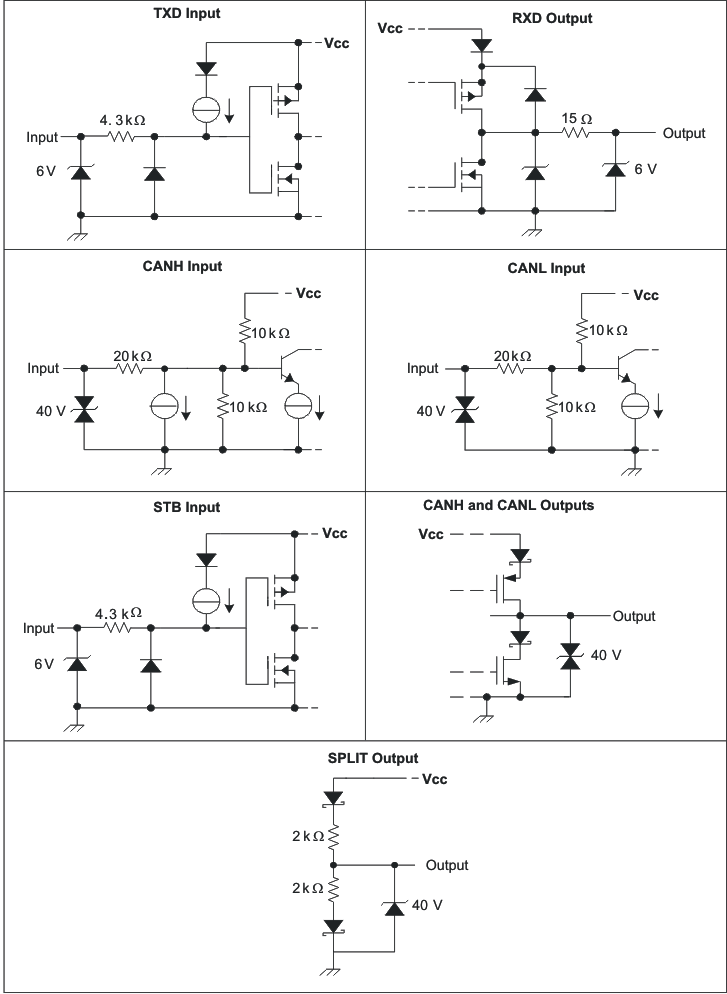
 Figure 24. Equivalent Input and Output Schematic Diagrams