SLLS889C June 2008 – August 2016 SN65HVD1040A-Q1
PRODUCTION DATA.
- 1 Features
- 2 Applications
- 3 Description
- 4 Revision History
- 5 Description (continued)
- 6 Pin Configuration and Functions
- 7 Specifications
- 8 Parameter Measurement Information
- 9 Detailed Description
- 10Application and Implementation
- 11Power Supply Recommendations
- 12Layout
- 13Device and Documentation Support
- 14Mechanical, Packaging, and Orderable Information
Package Options
Mechanical Data (Package|Pins)
- D|8
Thermal pad, mechanical data (Package|Pins)
Orderable Information
10 Application and Implementation
NOTE
Information in the following applications sections is not part of the TI component specification, and TI does not warrant its accuracy or completeness. TI’s customers are responsible for determining suitability of components for their purposes. Customers should validate and test their design implementation to confirm system functionality.
10.1 Application Information
10.1.1 Using With 3.3-V Microcontrollers
The input level threshold for the digital input pins of this device are 3.3-V compatible; however, a few application considerations must be taken if using this device with 3.3-V microcontrollers. Both TXD and STB input pins have internal pullup sources to VCC. Some microcontroller vendors recommend using an open-drain configuration on their I/O pins in this case even though the pullup limits the current. Take care of the application level so that TXD and STB have sufficient pullup to meet system timing requirements for CAN. The internal pullup on TXD especially may not be sufficient to overcome the parasitic capacitances and allow for adequate CAN timing; thus, an additional external pullup may be required. Also take care of the RXD pin of the microcontroller as the RXD output of this device drives the full VCC range (5 V). If the microcontroller RXD input pin is not 5-V tolerant, this must be addressed at the application level. Other options include using a CAN transceiver from TI with I/O level adapting or a 3.3-V CAN transceiver.
10.1.2 Using SPLIT With Split Termination
The SPLIT pin voltage output provides 0.5 × VCC in normal mode. The circuit may be used by the application to stabilized the common-mode voltage of the bus by connecting it to the center tap of split termination for the CAN network (see Figure 19 and Figure 20). This pin provides a stabilizing recessive voltage drive to offset leakage currents of unpowered transceivers or other bias imbalances that might bring the network common-mode voltage away from 0.5 × VCC. Using this feature in a CAN network improves electromagnetic emissions behavior of the network by eliminating fluctuations in the bus common-mode voltage levels at the start of message transmissions.
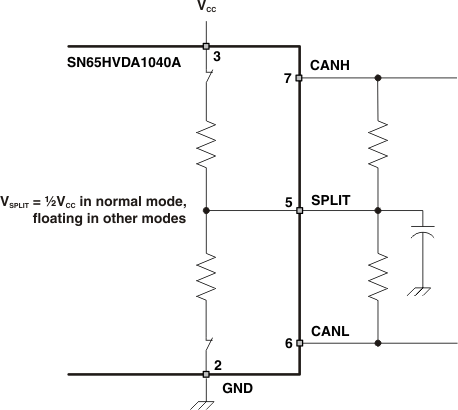 Figure 19. Split Pin Stabilization Circuitry and Application
10.2 Typical Application
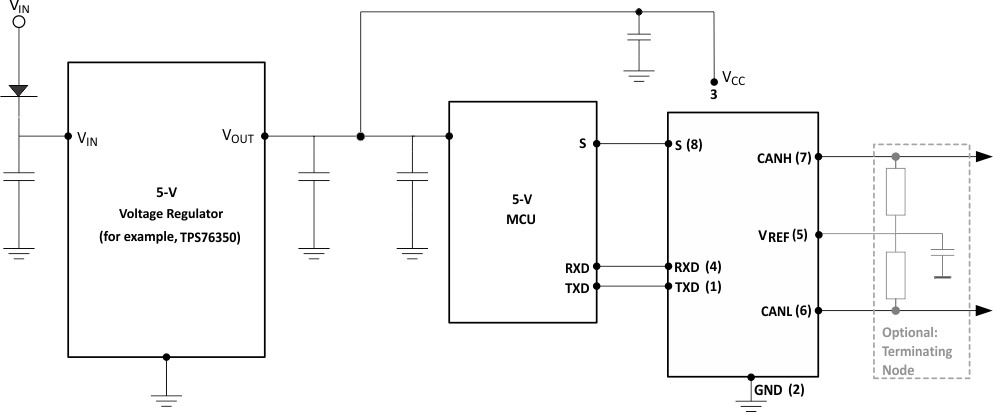 Figure 20. Typical Application Using Split Termination for Stabilization Diagram
10.2.1 Design Requirements
10.2.1.1 Bus Loading, Length, and Number of Nodes
The ISO 11898 Standard specifies up to 1-Mbps data rate, maximum bus length of 40 meters, maximum drop line (stub) length of 0.3 meters, and a maximum of 30 nodes. However, with careful network design, the system may have longer cables, longer stub lengths, and many more nodes to a bus. Many CAN organizations and standards have scaled the use of CAN for applications outside the original ISO 11898 standard. They have made system-level trade-offs for data rate, cable length, and parasitic loading of the bus. Examples of some of these specifications are ARINC825, CANopen, CAN Kingdom, DeviceNet, and NMEA200.
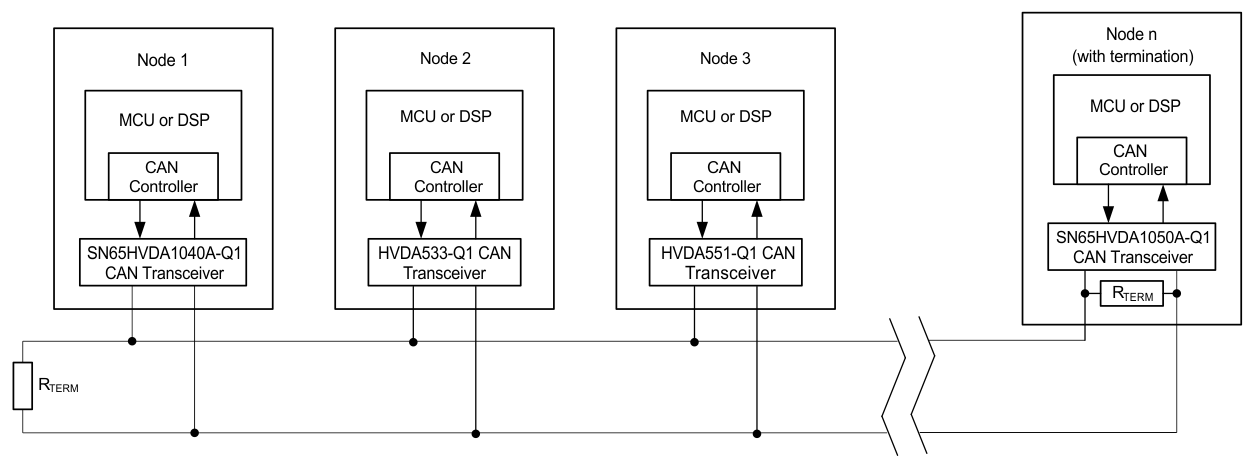 Figure 21. Typical CAN Bus Drawing
A high number of nodes requires a transceiver with high input impedance and wide common-mode range such as the SN65HVD1040A-Q1 CAN transceiver. ISO 11898-2 specifies the driver differential output with a 60-Ω load (two 120-Ω termination resistors in parallel) and the differential output must be greater than 1.5 V. The SN65HVD1040A-Q1 device is specified to meet the 1.5-V requirement with a 60-Ω load, and additionally specified with a differential output voltage minimum of 1.2 V across a common-mode range of –2 V to 7 V through a 330-Ω coupling network. This network represents the bus loading of 90 SN65HVD1040A-Q1 transceivers based on their minimum differential input resistance of 30 kΩ. Therefore, the SN65HVD1040A-Q1 supports up to 90 transceivers on a single bus segment with margin to the 1.2-V minimum differential input voltage requirement at each node.
For CAN network design, margin must be given for signal loss across the system and cabling, parasitic loadings, network imbalances, ground offsets, and signal integrity, thus a practical maximum number of nodes may be lower. Bus length may also be extended beyond the original ISO 11898 standard of 40 meters by careful system design and data rate tradeoffs. For example, CANopen network design guidelines allow the network to be up to 1-km with changes in the termination resistance, cabling, less than 64 nodes and significantly lowered data rate.
This flexibility in CAN network design is one of the key strengths of the various extensions and additional standards that have been built on the original ISO 11898 CAN standard.
10.2.1.2 CAN Termination
The ISO 11898 standard specifies the interconnect to be a twisted pair cable (shielded or unshielded) with 120-Ω characteristic impedance (ZO ). Resistors equal to the characteristic impedance of the line must be used to terminate both ends of the cable to prevent signal reflections. Unterminated drop lines (stubs) connecting nodes to the bus must be kept as short as possible to minimize signal reflections. The termination may be on the cable or in a node, but if nodes may be removed from the bus the termination must be carefully placed so that it is not removed from the bus.
Termination is typically a 120-Ω resistor at each end of the bus. If filtering and stabilization of the common-mode voltage of the bus is desired, then split termination may be used (see Figure 22 and Using SPLIT With Split Termination).
Take care when determining the power ratings of the termination resistors. A typical worst-case fault condition is if the system power supply and ground were shorted across the termination resistance which would result in much higher current through the termination resistance than the current limit of the CAN transceiver.
 Figure 22. CAN Termination Schematic
10.2.1.3 Loop Propagation Delay
Transceiver loop delay is a measure of the overall device propagation delay, consisting of the delay from the driver input (the TXD pin) to the differential outputs (the CANH and CANL pins), plus the delay from the receiver inputs (the CANH and CANL) to its output (the RXD pin). A typical loop delay for the SN65HVD1040A-Q1 transceiver is displayed in Figure 24 and Figure 25.
10.2.2 Detailed Design Procedure
10.2.2.1 Transient Voltage Suppresser (TVS) Diodes
Transient voltage suppressors are the preferred protection components for a CAN bus due to their low capacitance, which allows them to be designed into every node of a multinode network without requiring a reduction in data rate. With response times of a few picoseconds and power ratings of up to several kilowatts, TVS diodes present the most effective protection against ESD, burst, and surge transients.
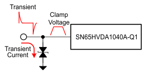 Figure 23. Transient Voltage Suppresser (TVS) Diodes Schematic
10.2.3 Application Curves
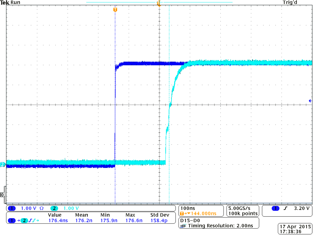
Dominant to Recessive
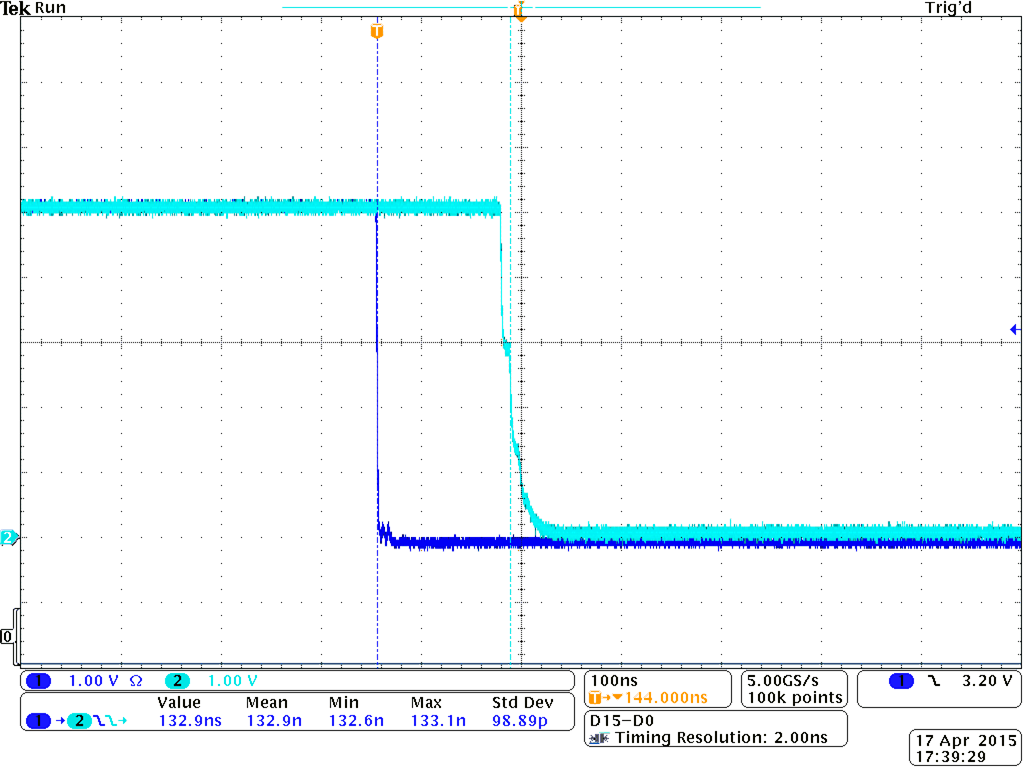
Recessive to Dominant