SLLS889C June 2008 – August 2016 SN65HVD1040A-Q1
PRODUCTION DATA.
- 1 Features
- 2 Applications
- 3 Description
- 4 Revision History
- 5 Description (continued)
- 6 Pin Configuration and Functions
- 7 Specifications
- 8 Parameter Measurement Information
- 9 Detailed Description
- 10Application and Implementation
- 11Power Supply Recommendations
- 12Layout
- 13Device and Documentation Support
- 14Mechanical, Packaging, and Orderable Information
Package Options
Mechanical Data (Package|Pins)
- D|8
Thermal pad, mechanical data (Package|Pins)
Orderable Information
12 Layout
12.1 Layout Guidelines
For the PCB design to be successful, start with design of the protection and filtering circuitry. Because ESD and EFT transients have a wide frequency bandwidth from approximately 3-MHz to 3-GHz, high-frequency layout techniques must be applied during PCB design. On-chip IEC ESD protection is good for laboratory and portable equipment but is usually not sufficient for EFT and surge transients occurring in industrial environments. Therefore, robust and reliable bus node design requires the use of external transient protection devices at the bus connectors. Placement at the connector also prevents these harsh transient events from propagating further into the PCB and system.
Use VCC and ground planes to provide low inductance.
NOTE
High-frequency current follows the path of least inductance and not the path of least resistance.
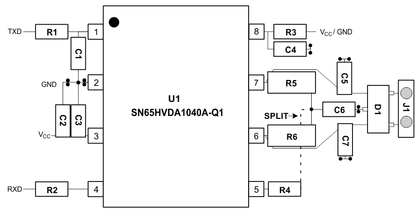
Design the bus protection components in the direction of the signal path. Do not force the transient current to divert from the signal path to reach the protection device. An example placement of the Transient Voltage Suppression (TVS) device indicated as D1 (either bidirectional diode or varistor solution) and bus filter capacitors C5 and C7 are shown in Figure 26.
The bus transient protection and filtering components must be placed as close to the bus connector, J1, as possible. This prevents transients, ESD and noise from penetrating onto the board and disturbing other devices.
Bus termination: Figure 22 shows split termination. This is where the termination is split into two resistors, R5 and R6, with the center or split tap of the termination connected to ground through capacitor C6. Split termination provides common-mode filtering for the bus. When termination is placed on the board instead of directly on the bus, take care to ensure the terminating node is not removed from the bus as this causes signal integrity issues if the bus is not properly terminated on both ends.
Bypass and bulk capacitors should be placed as close as possible to the supply pins of transceiver, examples include C2 and C3 (VCC ).
Use at least two vias for VCC and ground connections of bypass capacitors and protection devices to minimize trace and via inductance.
To limit current of digital lines, serial resistors may be used. Examples are R1, R2, R3, and R4.
To filter noise on the digital IO lines, a capacitor may be used close to the input side of the IO as shown by C1 and C4.
Because the internal pullup and pulldown biasing of the device is weak for floating pins, an external 1-kΩ to 10- kΩ pullup or pulldown resistor must be used to bias the state of the pin more strongly against noise during transient events.
Pin 1: If an open-drain host processor is used to drive the TXD pin of the device an external pullup resistor between 1 kΩ and 10 kΩ must be used to drive the recessive input state of the device.
Pin 5: SPLIT must be connected to the center point of a split termination scheme to help stabilize the common-mode voltage to VCC /2. If SPLIT is unused it must be left floating.
Pin 8: Is shown assuming the mode pin, STB, is used. If the device is only used in normal mode, R3 is not needed and the pads of C4 could be used for the pulldown resistor to GND.
12.2 Layout Example
 Figure 26. Typical CAN Bus Layout Example
12.3 ESD Protection
A typical application that employees a CAN bus network may require some form of ESD, burst, and surge protection to shield the CAN transceiver against unwanted transients that can potential damage the transceiver. To help shield the SN65HVD1040A-Q1 transceiver against these high-energy transients, transient voltage suppressors can be implemented on the CAN differential bus terminals. These devices help absorb the impact of a ESD, burst, or surge strike.