SLLS505P February 2002 – February 2022 SN65HVD10 , SN65HVD11 , SN65HVD12 , SN75HVD10 , SN75HVD11 , SN75HVD12
PRODUCTION DATA
- 1 Features
- 2 Applications
- 3 Description
- 4 Revision History
- 5 Device Comparison Table
- 6 Pin Configuration and Functions
-
7 Specifications
- 7.1 Absolute Maximum Ratings
- 7.2 ESD Ratings
- 7.3 Recommended Operating Conditions
- 7.4 Thermal Information
- 7.5 Driver Electrical Characteristics
- 7.6 Receiver Electrical Characteristics
- 7.7 Power Dissipation Characteristics
- 7.8 Driver Switching Characteristics
- 7.9 Receiver Switching Characteristics
- 7.10 Dissipation Ratings
- 7.11 Typical Characteristics
- 8 Parameter Measurement Information
- 9 Detailed Description
- 10Application and Implementation
- 11Power Supply Recommendations
- 12Layout
- 13Device and Documentation Support
- 14Mechanical, Packaging, and Orderable Information
Package Options
Mechanical Data (Package|Pins)
Thermal pad, mechanical data (Package|Pins)
Orderable Information
7.11 Typical Characteristics
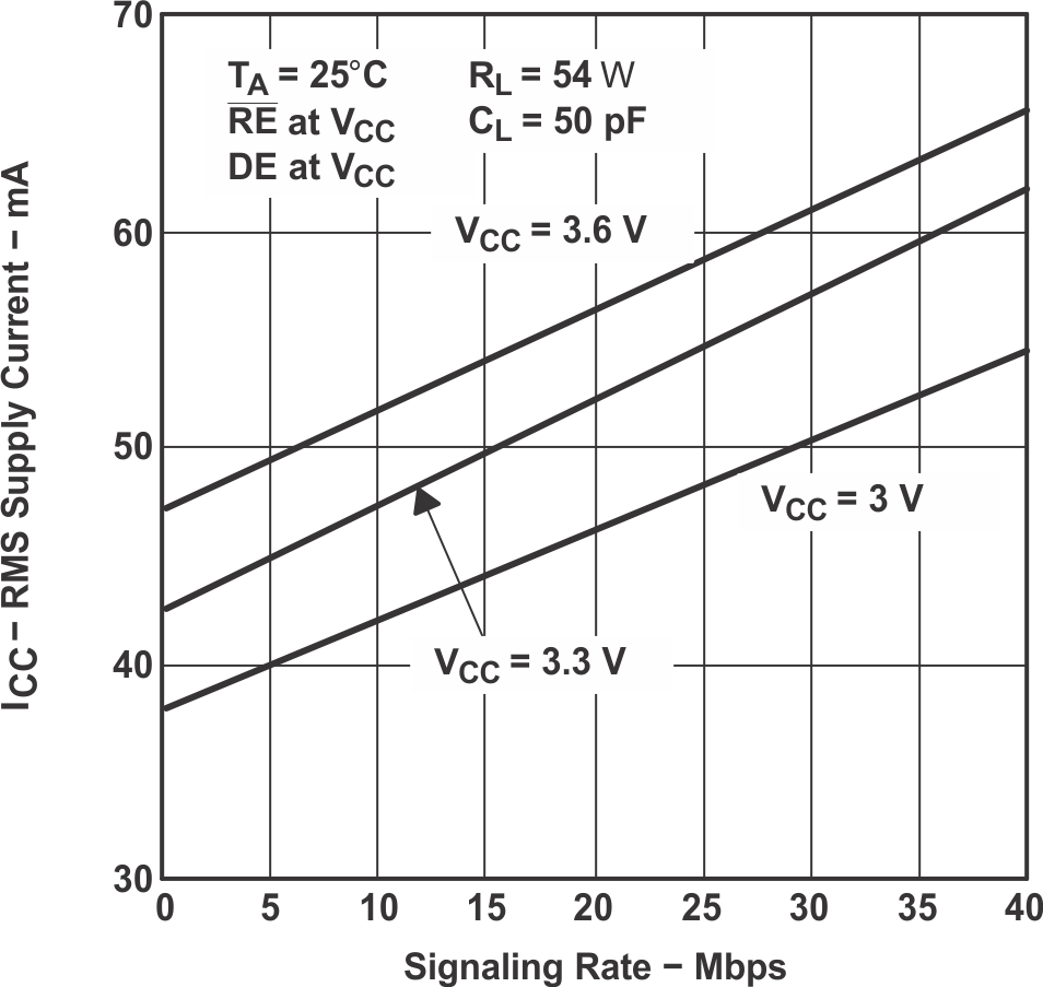 Figure 7-1 HVD10 RMS Supply Current vs Signaling Rate
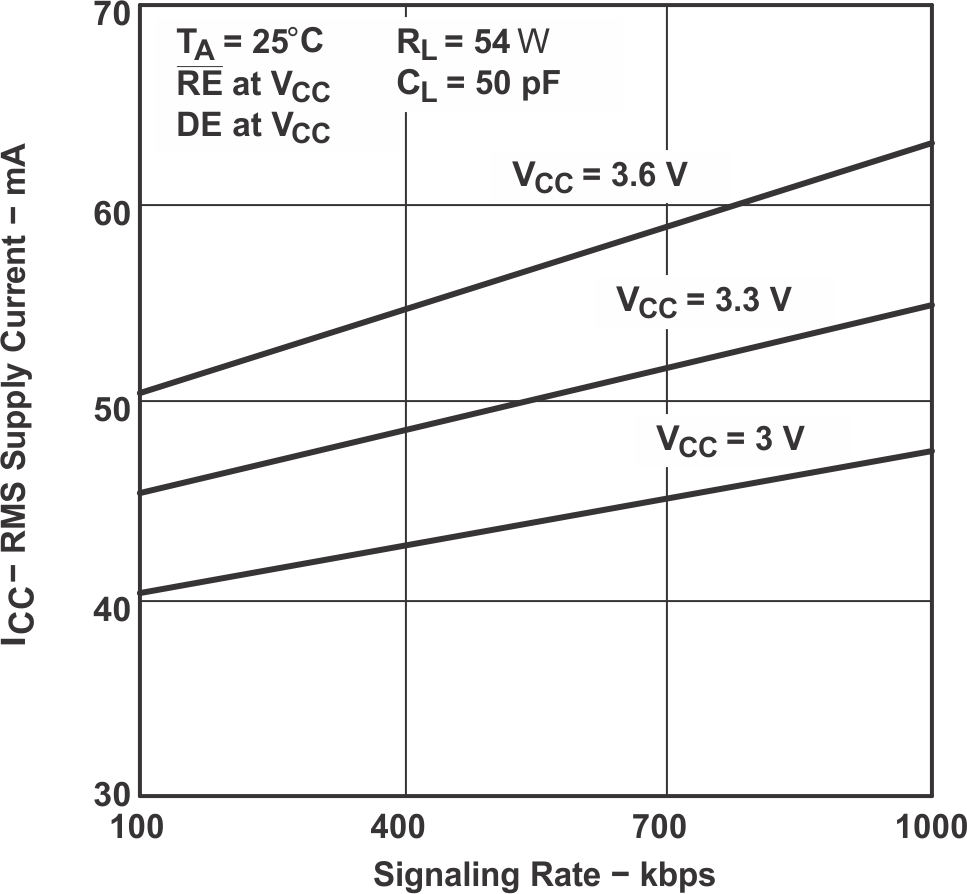 Figure 7-3 HVD12 RMS Supply Current vs Signaling Rate
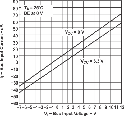 Figure 7-5 HVD11 or HVD12 Bus Input Current vs Bus Input Voltage
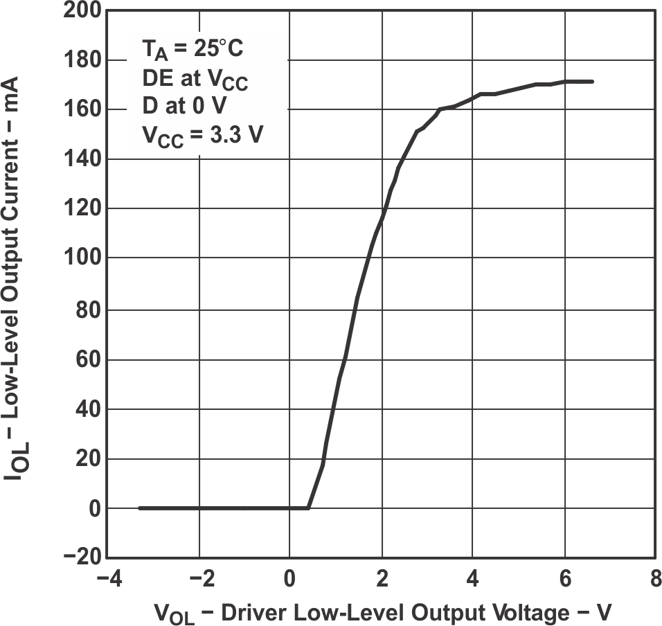 Figure 7-7 Low-Level Output Current vs Driver Low-Level Output Voltage
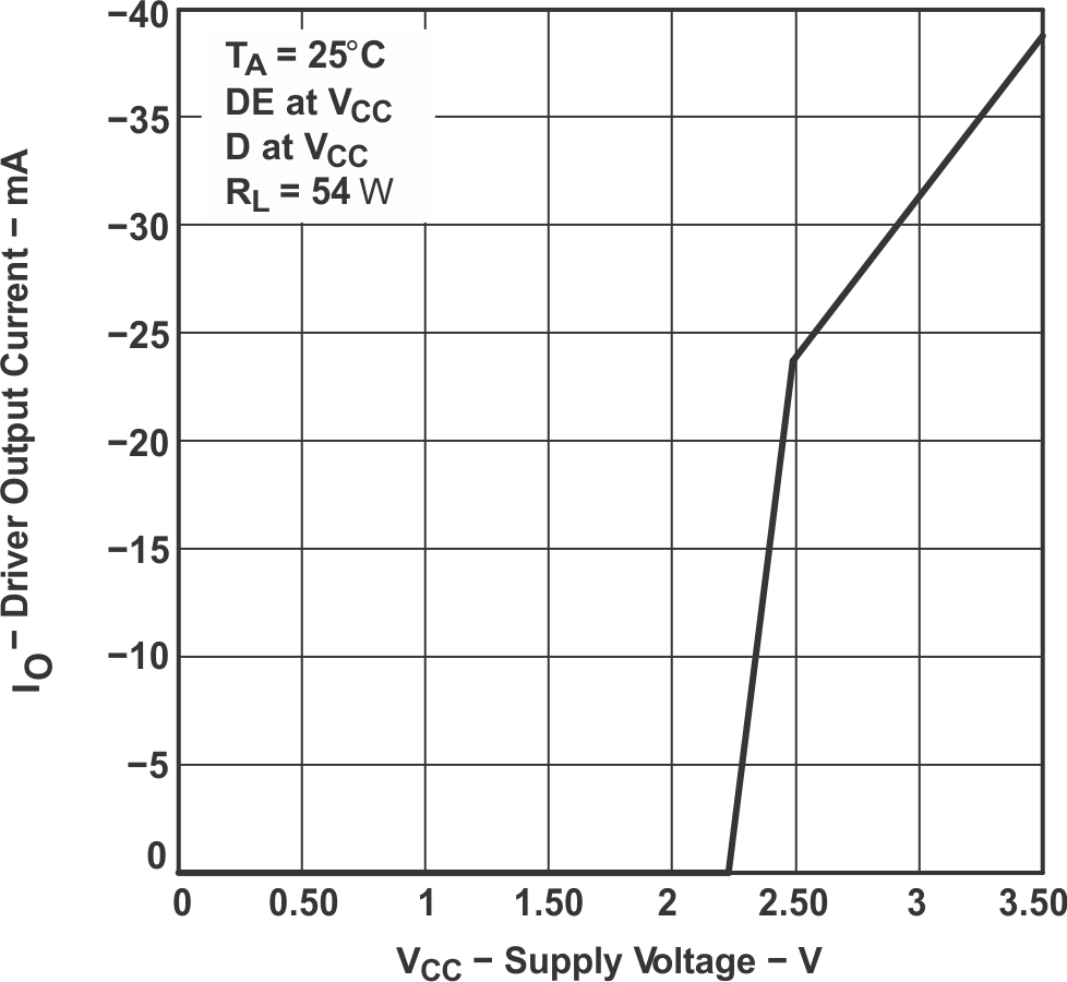 Figure 7-9 Driver Output Current vs Supply Voltage
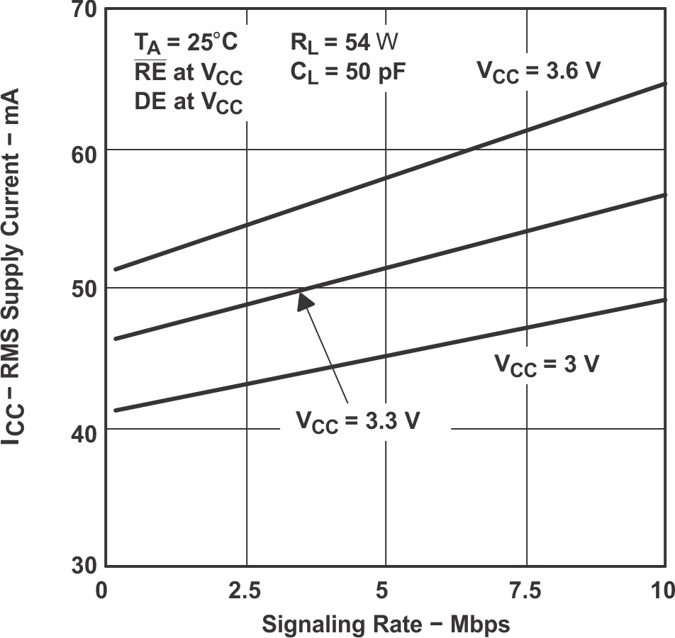 Figure 7-2 HVD11 RMS Supply Current vs Signaling Rate
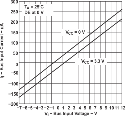 Figure 7-4 HVD10 Bus Input Current vs Bus Input Voltage
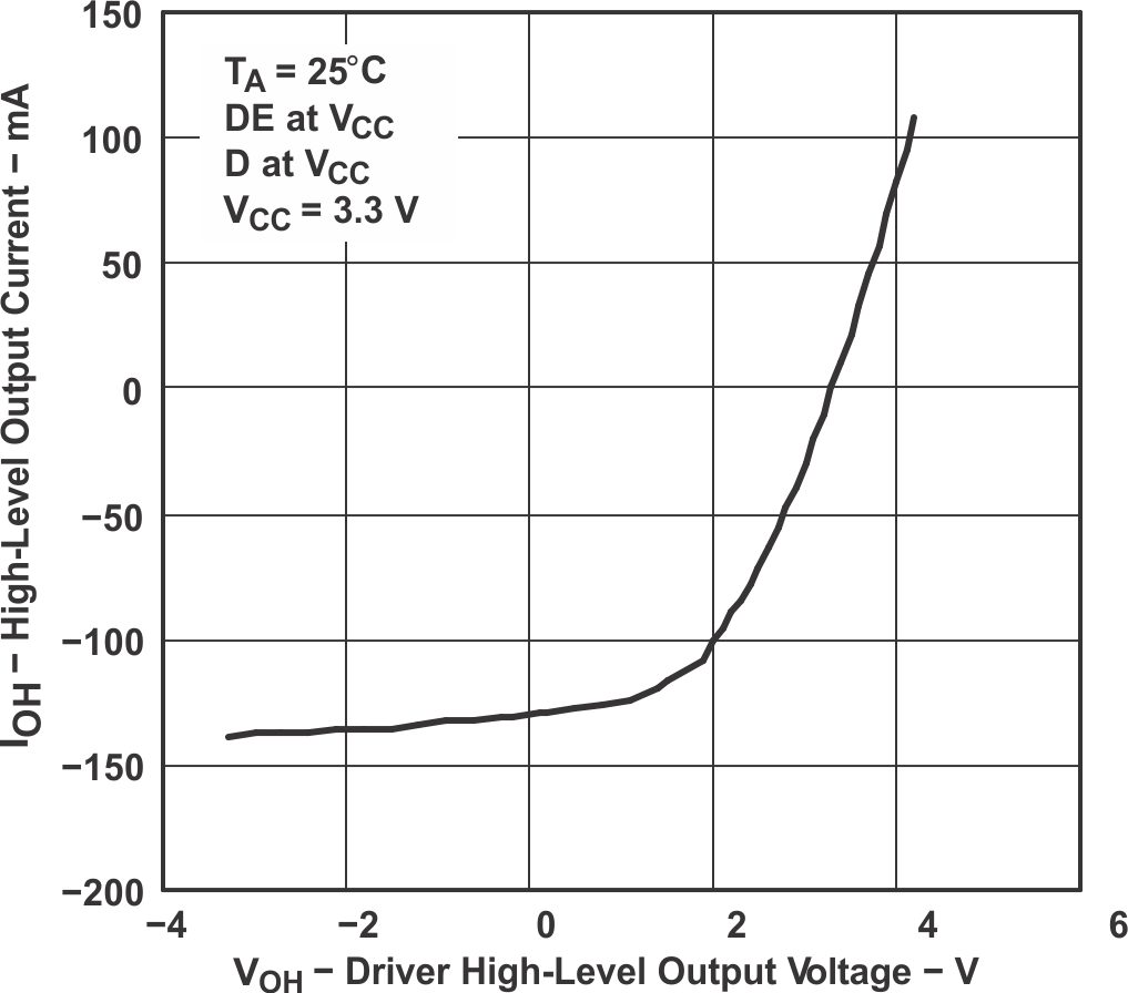 Figure 7-6 High-Level Output Current vs Driver High-Level Output Voltage
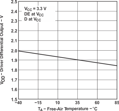 Figure 7-8 Driver Differential Output vs Free-Air Temperature
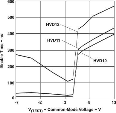 Figure 7-10 Enable Time vs Common-Mode Voltage