SLLS505P February 2002 – February 2022 SN65HVD10 , SN65HVD11 , SN65HVD12 , SN75HVD10 , SN75HVD11 , SN75HVD12
PRODUCTION DATA
- 1 Features
- 2 Applications
- 3 Description
- 4 Revision History
- 5 Device Comparison Table
- 6 Pin Configuration and Functions
-
7 Specifications
- 7.1 Absolute Maximum Ratings
- 7.2 ESD Ratings
- 7.3 Recommended Operating Conditions
- 7.4 Thermal Information
- 7.5 Driver Electrical Characteristics
- 7.6 Receiver Electrical Characteristics
- 7.7 Power Dissipation Characteristics
- 7.8 Driver Switching Characteristics
- 7.9 Receiver Switching Characteristics
- 7.10 Dissipation Ratings
- 7.11 Typical Characteristics
- 8 Parameter Measurement Information
- 9 Detailed Description
- 10Application and Implementation
- 11Power Supply Recommendations
- 12Layout
- 13Device and Documentation Support
- 14Mechanical, Packaging, and Orderable Information
Package Options
Mechanical Data (Package|Pins)
Thermal pad, mechanical data (Package|Pins)
Orderable Information
3 Description
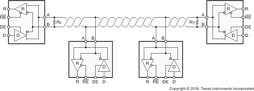
The SN65HVD10, SN75HVD10, SN65HVD11, SN75HVD11, SN65HVD12, and SN75HVD12 bus transceivers all combine a 3-state differential line driver, as well as a differential input line receiver that operates with a single 3.3-V power supply. They are designed for balanced transmission lines and meet or exceed ANSI standard TIA/EIA-485-A and ISO 8482:1993. These differential bus transceivers are monolithic integrated circuits, designed for bidirectional data communication on multipoint bus-transmission lines. The drivers and receivers have active-high and active-low enables, that can be externally connected together to function as direction control. Very low device standby supply current, can be achieved by disabling the driver and the receiver.
The driver differential outputs and receiver differential inputs connect internally to form a differential input/output (I/O) bus port, that is designed to offer minimum loading to the bus whenever the driver is disabled or VCC = 0. These parts feature wide positive and negative common-mode voltage ranges, making them suitable for party-line applications.
| PART NUMBER | PACKAGE(1) | BODY SIZE (NOM) |
|---|---|---|
| SN65HVD10 | SOIC (8) | 4.90 mm × 3.91 mm |
| SN65HVD11 | ||
| SN65HVD12 | ||
| SN75HVD10 | PDIP (8) | 9.81 mm × 6.35 mm |
| SN75HVD11 | ||
| SN75HVD12 |
 Typical Application Diagram