SLLSE49E September 2010 – October 2024 SN65HVD1780-Q1 , SN65HVD1781-Q1 , SN65HVD1782-Q1
PRODUCTION DATA
- 1
- 1 Features
- 2 Applications
- 3 Description
- 4 Pin Configuration and Functions
- 5 Specifications
- 6 Parameter Measurement Information
- 7 Detailed Description
- 8 Application and Implementation
- 9 Device and Documentation Support
- 10Revision History
- 11Mechanical, Packaging, and Orderable Information
Package Options
Mechanical Data (Package|Pins)
- D|8
Thermal pad, mechanical data (Package|Pins)
Orderable Information
8.2.2.2 Receiver Failsafe
The differential receivers of the SN65HVD178x-Q1 family have receiver input thresholds that are offset, so the receiver output state is known for the following three fault conditions:
- Open bus conditions, such as a disconnected connector
- Shorted bus conditions, such as cable damage shorting the twisted-pair together
- Idle bus conditions that occur when no driver on the bus is actively driving
In any of these cases, the differential receiver outputs a failsafe logic High state, so the output of the receiver is not indeterminate.
Receiver failsafe is accomplished by offsetting the receiver thresholds such that the input indeterminate range does not include zero volts differential. To comply with the RS-422 and RS-485 standards, the receiver output must output a High when the differential input VID is more positive than 200mV, and must output a Low when VID is more negative than –200mV. The receiver parameters which determine the failsafe performance are VIT(+), VIT(–), and VHYS (the separation between VIT(+) and VIT(–)). As shown in the Electrical Characteristics table, differential signals more negative than –200mV always cause a Low receiver output, and differential signals more positive than 200mV always cause a High receiver output.
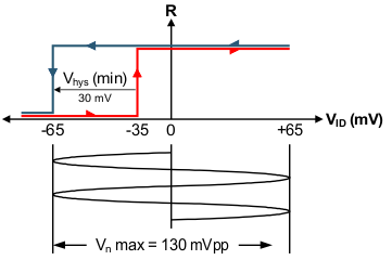
When the differential input signal is close to zero, the signal is still above the maximum VIT(+) threshold of –35 mV, and the receiver output is High. Only when the differential input is more than VHYS below VIT(+) does the receiver output transition to a Low state. Therefore, the noise immunity of the receiver inputs during a bus fault condition includes the receiver hysteresis value, VHYS, as well as the value of VIT(+).
 Figure 8-5 Noise Immunity Under Bus Fault Conditions