SLLS933G November 2008 – January 2015 SN65HVD233-HT
PRODUCTION DATA.
- 1 Features
- 2 Applications
- 3 Description
- 4 Revision History
- 5 Description (Continued)
- 6 Pin Configuration and Functions
-
7 Specifications
- 7.1 Absolute Maximum Ratings
- 7.2 ESD Ratings
- 7.3 Recommended Operating Conditions
- 7.4 Thermal Information
- 7.5 Driver Electrical Characteristics
- 7.6 Receiver Electrical Characteristics
- 7.7 Driver Switching Characteristics
- 7.8 Receiver Switching Characteristics
- 7.9 Device Switching Characteristics
- 7.10 Typical Characteristics
- 8 Parameter Measurement Information
- 9 Detailed Description
- 10Application and Implementation
- 11Power Supply Recommendations
- 12Layout
- 13Device and Documentation Support
- 14Mechanical, Packaging, and Orderable Information
Package Options
Mechanical Data (Package|Pins)
Thermal pad, mechanical data (Package|Pins)
Orderable Information
9 Detailed Description
9.1 Overview
Controller Area Network (CAN) is a robust multi master-master, differential signaling, serial communications bus specified by the ISO 11898 family of standards. TI's SSN65HVD23x family of transceivers solve specialized networking requirements for various applications.
Table 2. Available Options
| ORDERABLE PART NUMBER | LOW-POWER MODE | SLOPE CONTROL |
DIAGNOSTIC LOOPBACK |
AUTOBAUD LOOPBACK |
|---|---|---|---|---|
| SN65HVD233HD | 200-μA standby mode | Adjustable | Yes | No |
| SN65HVD233SJD | ||||
| SN65HVD233SKGDA | ||||
| SN65HVD233SHKJ | ||||
| SN65HVD233SHKQ |
9.2 Functional Block Diagram

9.3 Feature Description
9.3.1 ISO 11898 Compliance of SN65HVD23x Family of 3.3-V CAN Transceivers
Many users value the low power consumption of operating CAN transceivers from a 3.3-V supply. However, some are concerned about the interoperability with 5-V supplied transceivers on the same bus. This section analyzes this situation to address those concerns.
9.3.1.1 Differential Signal
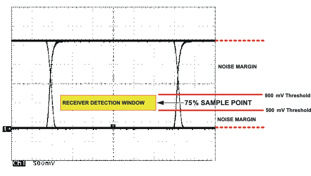
CAN is a differential bus where complementary signals are sent over two wires, and the voltage difference between the two wires defines the logical state of the bus. The differential CAN receiver monitors this voltage difference and outputs the bus state with a single-ended output signal.
 Figure 26. Typical SN65HVD23x Differential Output Voltage Waveform
The CAN driver creates the difference voltage between CANH and CANL in the dominant state. The dominant differential output of the SN65HVD23x is greater than 1.5 V and less than 3 V across a 60-Ω load. The minimum required by ISO 11898 is 1.5 V and the maximum is 3 V. These are the same limiting values for 5-V supplied CAN transceivers. The bus termination resistors drive the recessive bus state and not the CAN driver.
A CAN receiver is required to output a recessive state with less than 500 mV and a dominant state with more than 900-mV difference voltage on its bus inputs. The CAN receiver must do this with common-mode input voltages from –2 V to 7 V. The SN65HVD23x family receivers meet these same input specifications as 5-V supplied receivers.
9.3.1.1.1 Common-Mode Signal
A common-mode signal is an average voltage of the two signal wires that the differential receiver rejects. The common-mode signal comes from the CAN driver, ground noise, and coupled bus noise. Obviously, the supply voltage of the CAN transceiver has nothing to do with noise. The SN65HVD23x family driver lowers the common-mode output in a dominant bit by a couple hundred millivolts from that of most 5-V drivers. While this does not fully comply with ISO 11898, this small variation in the driver common-mode output is rejected by differential receivers and does not affect data, signal noise margins, or error rates.
9.3.1.2 Interoperability Of 3.3-V CAN in 5-V CAN Systems
The 3.3-V–supplied SN65HVD23x family of CAN transceivers are electrically interchangeable with 5-V CAN transceivers. The differential output is the same. The recessive common-mode output is the same. The dominant common-mode output voltage is a couple hundred millivolts lower than 5-V–supplied drivers, while the receivers exhibit identical specifications as 5-V devices.
Electrical interoperability does not assure interchangeability however. Most implementers of CAN buses recognize that ISO 11898 does not sufficiently specify the electrical layer and that strict standard compliance alone does not ensure interchangeability. This comes only with thorough equipment testing.
9.4 Device Functional Modes
9.4.1 Function Tables
Table 3. Function Table (Driver)(1)
| DRIVER | |||||
|---|---|---|---|---|---|
| INPUTS | OUTPUTS | ||||
| D | LBK | Rs | CANH | CANL | BUS STATE |
| X | X | >0.75 VCC | Z | Z | Recessive |
| L | L or open | ≤0.33 VCC | H | L | Dominant |
| H or open | X | Z | Z | Recessive | |
| X | H | ≤0.33 VCC | Z | Z | Recessive |
Table 4. Function Table (Receiver)
| RECEIVER | ||||
|---|---|---|---|---|
| INPUTS | OUTPUT | |||
| BUS STATE | VID = V(CANH) – V(CANL) | LBK | D | R |
| Dominant | VID ≥ 0.9 V | L or open | X | L |
| Recessive | VID ≤ 0.5 V or open | L or open | H or open | H |
| ? | 0.5 V < VID < 0.9 V | L or open | H or open | |
| X | X | H | L | L |
| X | X | H | H | |
9.4.2 Equivalent Input and Output Schematic Diagrams
 Figure 27. D Input
 Figure 29. CANH Input
 Figure 31. CANH and CANL Outputs
 Figure 33. LBK Input
 Figure 28. RS Input
 Figure 30. CANL Input
 Figure 32. R Output