SLLS666F September 2005 – March 2023 SN65HVD50 , SN65HVD51 , SN65HVD52 , SN65HVD53 , SN65HVD54 , SN65HVD55
PRODUCTION DATA
- 1 Features
- 2 Applications
- 3 Description
- 4 Revision History
- 5 Available Options
- 6 Pin Configurations
-
7 Specifications
- 7.1 Absolute Maximum Ratings
- 7.2 Recommended Operating Conditions
- 7.3 Electrostatic Discharge Protection
- 7.4 Driver Electrical Characteristics
- 7.5 Driver Switching Characteristics
- 7.6 Receiver Electrical Characteristics
- 7.7 Receiver Switching Characteristics
- 7.8 Thermal Characteristics
- 7.9 Typical Characteristics
- 8 Parameter Measurement Information
- 9 Device Information
- 10Application and Implementation
- 11Device and Documentation Support
- 12Mechanical, Packaging, and Orderable Information
Package Options
Mechanical Data (Package|Pins)
- D|14
Thermal pad, mechanical data (Package|Pins)
Orderable Information
8 Parameter Measurement Information
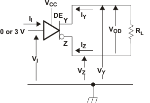 Figure 8-1 Driver
VOD Test Circuit: Voltage and Current Definitions
 Figure 8-2 Driver
VOD With Common-Mode Loading Test Circuit
Figure 8-2 Driver
VOD With Common-Mode Loading Test CircuitVOD(RING) is measured at four points on the output waveform, corresponding to overshoot and undershoot from the VOD(H) and VOD(L) steady state values.
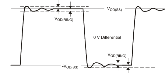 Figure 8-3 VOD(RING) Waveform and Definitions
 Figure 8-4 Test
Circuit and Definitions for the Driver Common-Mode Output Voltage
 Figure 8-5 Driver
Switching Test Circuit and Voltage Waveforms
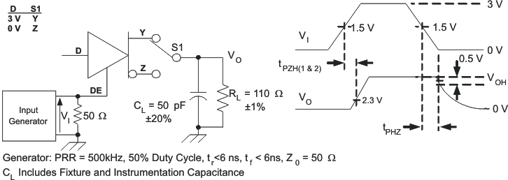 Figure 8-6 Driver
High-Level Output Enable and Disable Time Test Circuit and Voltage
Waveforms
 Figure 8-7 Driver
Low-Level Output Enable and Disable Time Test Circuit and Voltage
Waveforms
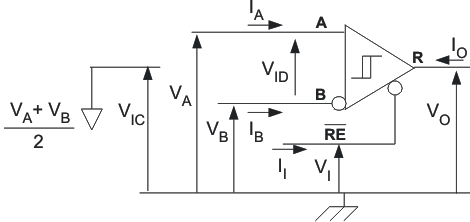 Figure 8-8 Receiver
Voltage and Current Definitions
 Figure 8-9 Receiver
Switching Test Circuit and Voltage Waveforms
 Figure 8-10 Receiver
High-Level Enable and Disable Time Test Circuit and Voltage Waveforms
 Figure 8-11 Receiver
Low-Level Enable and Disable Time Test Circuit and Voltage Waveforms
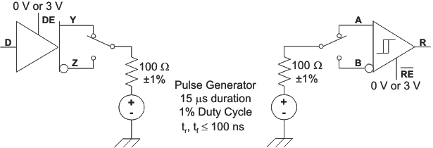 Figure 8-12 Test
Circuit, Transient Overvoltage Test