SLLSE94C September 2011 – March 2015 SN65HVD62
PRODUCTION DATA.
- 1 Features
- 2 Applications
- 3 Description
- 4 Block Diagram
- 5 Revision History
- 6 Pin Configuration and Functions
- 7 Specifications
- 8 Parameter Measurement Information
- 9 Detailed Description
- 10Application and Implementation
- 11Device and Documentation Support
- 12Mechanical, Packaging, and Orderable Information
Package Options
Mechanical Data (Package|Pins)
- RGT|16
Thermal pad, mechanical data (Package|Pins)
- RGT|16
Orderable Information
7 Specifications
7.1 Absolute Maximum Ratings(1)
| VALUES | UNIT | ||
|---|---|---|---|
| MIN | MAX | ||
| Supply voltage, VCC and VL | –0.5 | 6 | V |
| Voltage range at coax pins | –0.5 | 6 | V |
| Voltage range at logic pins | –0.3 | VL + 0.3 | V |
| Logic Output Current | –20 | 20 | mA |
| TXOUT output current | Internally limited | ||
| SYNCOUT output current | Internally limited | ||
| Junction Temperature, TJ | 170 | °C | |
| Storage temperature, TSTG | –65 | 150 | |
| Continuous total power dissipation | See the Thermal Information | °C | |
(1) Stresses beyond those listed under “absolute maximum ratings” may cause permanent damage to the device. These are stress ratings only and functional operation of the device at these or any other conditions beyond those indicated under “recommended operating conditions” is not implied. Exposure to absolute-maximum-rated conditions for extended periods may affect device reliability.
7.2 ESD Ratings
| VALUE | UNIT | |||
|---|---|---|---|---|
| V(ESD) | Electrostatic discharge | Human-body model (HBM), per ANSI/ESDA/JEDEC JS-001(1) | ±2000 | V |
(1) JEDEC document JEP155 states that 500-V HBM allows safe manufacturing with a standard ESD control process.
7.3 Thermal Information
| THERMAL METRIC(1) | SN65HVD62 | UNIT | |
|---|---|---|---|
| RGT (VQFN) | |||
| (16) PINS | |||
| RθJA | Junction-to-ambient thermal resistance | 49.4 | °C/W |
| RθJCtop | Junction-to-case (top) thermal resistance | 64.2 | |
| RθJB | Junction-to-board thermal resistance | 22.9 | |
| ψJT | Junction-to-top characterization parameter | 1.7 | |
| ψJB | Junction-to-board characterization parameter | 22.9 | |
| RθJCbot | Junction-to-case (bottom) thermal resistance | 25.0 | |
(1) For more information about traditional and new thermal metrics, see the IC Package Thermal Metrics application report, SPRA953.
7.4 Recommended Operating Conditions
7.5 Electrical Characteristics
over recommended operating conditions (unless otherwise noted)| PARAMETER | TEST CONDITIONS | MIN | TYP | MAX | UNIT | |||
|---|---|---|---|---|---|---|---|---|
| POWER SUPPLY | ||||||||
| 100 | ICC | Supply current (VCC) | TXIN = L (Active) | DIRSET1 = L DIRSET2 = H |
28 | 33 | mA | |
| 101 | TXIN = H (Quiescent) | 25 | 31 | |||||
| 102 | TXIN = 115 kbps, 50% duty cycle |
27 | 33 | |||||
| 99 | (Standby) DIRSET1 = DIRSET2=H | 12 | 17 | |||||
| 103 | IL | Logic supply current | TXIN = H, RXIN = DC input | 50 | µA | |||
| 104 | ΔVRXIN/ ΔVCC |
Receiver power supply rejection ratio | VTXIN = VL | 45 | 60 | dB | ||
| LOGIC PINS | ||||||||
| 112 | VOH | High-level logic output voltage (RXOUT, DIR) |
IOH = –4 mA for VL > 2.4V, IOH = –2 mA for VL < 2.4V |
90%VL | V | |||
| 113 | VOL | Low-level logic output voltage (RXOUT, DIR) |
IOL = 4 mA for VL > 2.4V, IOL = 2 mA for VL < 2.4V |
10%VL | V | |||
| 114 | IIH/IIL | Logic input current (DIRSET1/2) | -1 | 10 | µA | |||
| IIH/IIL | Logic input current (TXIN) | -2 | 1 | µA | ||||
| COAX DRIVER | ||||||||
| 130 | VOPP | Peak-to-peak output voltage at device pin TXOUT (See Figure 19) | VRES = 1.5 V (Maximum setting) | 2.24 | 2.5 | VPP | ||
| 132 | VRES = 0.7 V (Minimum setting) | 1.17 | 1.3 | |||||
| 130A | VOPP | Peak-to-peak voltage at coax out (See Figure 19) | VRES = 1.5 V | 5 | 6 | dBm | ||
| 132A | VRES = 0.7 V | -0.6 | 0.3 | |||||
| 134 | VOZ | Off-state output voltage | At TXOUT | 1 | mVpp | |||
| 134A | At coax out | -60 | dBm | |||||
| 136 | Output emissions | Coupled to coaxial cable with characteristic impedance 50 Ohms, as shown in Figure 1. With a recommended 470 pF capacitor between RXIN and GND. Measurements above 150 MHz are determined by setup. | Conforms to AISG spectrum emissions mask, 3GPP TS 25.461, see Figure 21 | |||||
| 41 | fo | Output frequency (HVD62) | 2.176 | MHz | ||||
| 142 | ∆f | Output frequency variation | –100 | 100 | ppm | |||
| 143 | Zo | Output impedance | At 100 kHz | 0.03 | Ω | |||
| 144 | At 10 MHz | 3.5 | Ω | |||||
| 145 | | IOS | | Short-circuit output current | TXOUT is also protected by a thermal shutdown circuit during short-circuit faults | 300 | 450 | mA | ||
| COAX RECEIVER | ||||||||
| 152 | VIT | Input threshold | fIN = 2.176 MHz | 79 | 112 | 158 | mVPP | |
| 152A | –18 | –15 | –12 | dBm | ||||
| 154 | ZIN | Input impedance | f = fO | 11 | 21 | kΩ | ||
| RECEIVER FILTER | ||||||||
| 160 | fPB | Passband | VRXIN = 1.12VP_P | 1.1 | 4.17 | MHz | ||
| 161 | fREJ | Receiver rejection range | 2.176MHz carrier amplitude of 112.4 mVPP, Frequency band of spurious components with 800 mVPP allowed. | 1.1 | 4.17 | MHz | ||
| 162 | tnoise filter | Receiver noise filter time (slow bit rate) | DIRSET for 9.6kbps | 4 | µs | |||
| 163 | Receiver noise filter time (fast bit rate) | DIRSET for > 9.6 kbps | 2 | |||||
| XTAL AND SYNC | ||||||||
| 171 | II | Input leakage current | XTAL1, XTAL2, 0V < VIN < VCC | –15 | 15 | µA | ||
| 172 | VOL | Output low voltage | SYNCOUT, with 1 kΩ resistor from SYNCOUT to VCC | 0.4 | V | |||
7.6 Switching Characteristics
over recommended operating conditions (unless otherwise noted)| PARAMETER | TEST CONDITIONS | MIN | TYP | MAX | UNIT | ||
|---|---|---|---|---|---|---|---|
| 201 | tpAQ, tpQA | Coax driver propagation delay | See Figure 19 | 5 | µs | ||
| 202 | tr, tf | Coax receiver output rise/fall time | CL = 15 pF, RL = 1 kΩ, See Figure 19 | 20 | ns | ||
| 203 | tPHL, tPLH | Receiver propagation delay | See Figure 20 | 5.5 | 11 | µs | |
| 204 | Duty Cycle | Coax receiver output duty cycle | VRXIN(ON) = 630 mVpp, VRXIN(OFF) < 5 mVpp, 50% duty cycle | 40% | 60% | ||
| 214 | VRXIN(ON) = 200 mVpp, VRXIN(OFF) < 5 mVpp, 50% duty cycle | 40% | 60% | ||||
| 206 | tDIR | Direction control active duration | DIRSET2 = DIRSET1 = GND or OPEN | 1667 | µs | ||
| 207 | DIRSET2 = GND, DIRSET1 = VL | 417 | |||||
| 208 | DIRSET2 = VL, DIRSET1 = VL | 137 | |||||
| 209 | tDIR Skew | Direction control skew (DIR to RXOUT) |
270 | ns | |||
| 210 | tDIS | Standby disable delay | 300 mVPP at 2.176 MHz on RXIN | 2 | ms | ||
| 211 | tEN | Standby enable delay | 2 |
7.7 Typical Characteristics
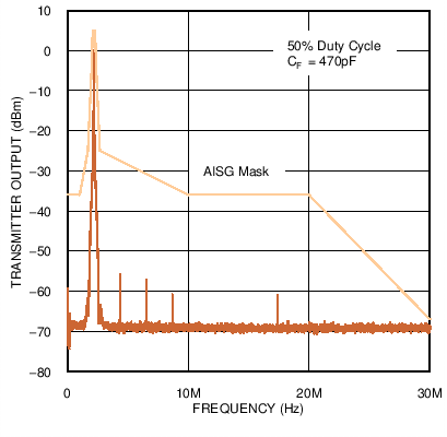 Figure 1. Low Frequency Emissions Spectrum with 9.6 kbps Signaling Rate
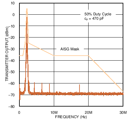 Figure 3. Low Frequency Emissions Spectrum with 38.4 kbps Signaling Rate
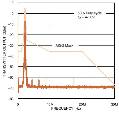 Figure 5. Low Frequency Emissions Spectrum with 115.2 kbps Signaling Rate
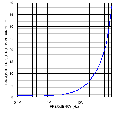 Figure 7. Transmitter Output Impedance
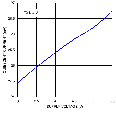 Figure 9. Supply Current versus Supply Voltage while Transmitting
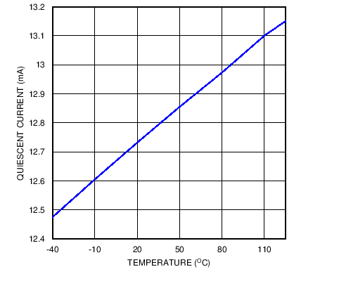 Figure 11. Supply Current versus Temperature in Standby Mode
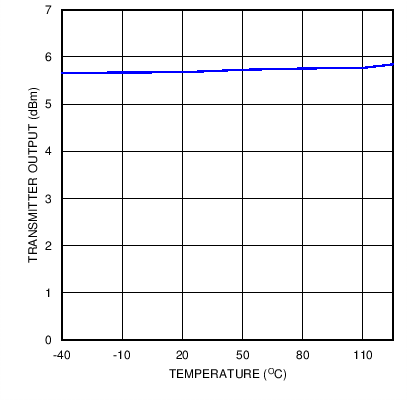 Figure 13. Transmitter Output Power versus Temperature
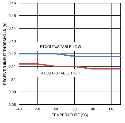 Figure 15. Receiver Input Threshold versus Temperature
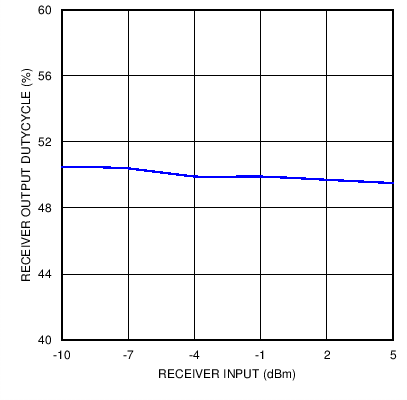 Figure 17. Receiver Duty Cycle with 9.6 kbps Signaling Rate
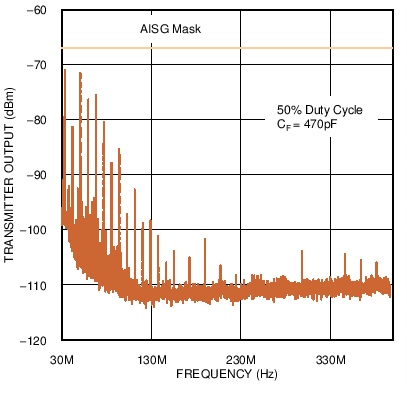 Figure 2. High Frequency Emissions Spectrum with 9.6 kbps Signaling Rate
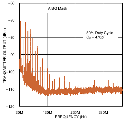 Figure 4. High Frequency Emissions Spectrum with 38.4 kbps Signaling Rate
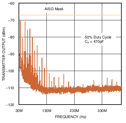 Figure 6. High Frequency Emissions Spectrum with 115.2 kbps Signaling Rate
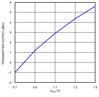 Figure 8. Transmit Power Adjustment
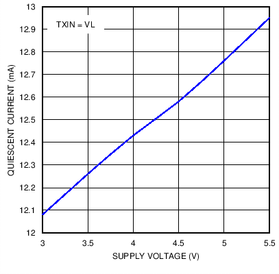 Figure 10. Supply Current versus Supply Voltage in Standby Mode
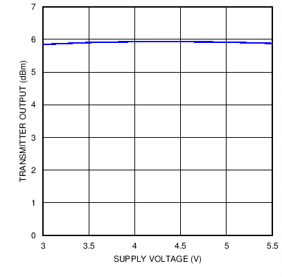 Figure 12. Transmitter Output Power versus Supply Voltage
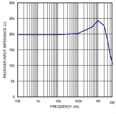 Figure 14. Receiver Input Impedance versus Frequency
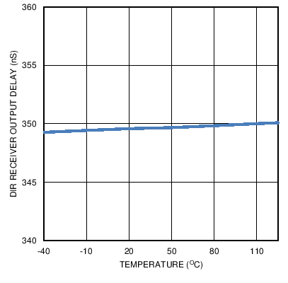 Figure 16. DIR Output Delay versus Temperature
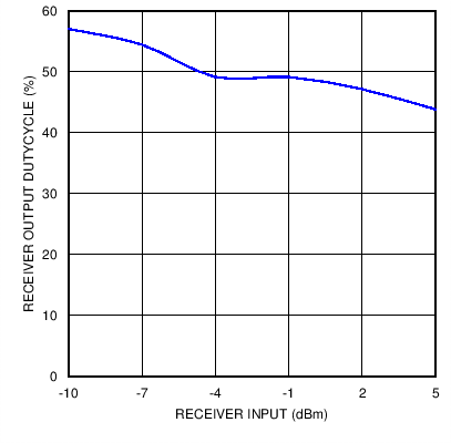 Figure 18. Receiver Duty Cycle with 115.2 kbps Signaling Rate