SLLSFI7 October 2020 SN65HVD64
PRODUCTION DATA
- 1 Features
- 2 Applications
- 3 Description
- 4 Revision History
- 5 Pin Configuration and Functions
- 6 Specifications
- 7 Parameter Measurement Information
- 8 Detailed Description
- 9 Application and Implementation
- 10Power Supply Recommendations
- 11Layout
- 12Device and Documentation Support
Package Options
Mechanical Data (Package|Pins)
- RGT|16
Thermal pad, mechanical data (Package|Pins)
- RGT|16
Orderable Information
5 Pin Configuration and Functions
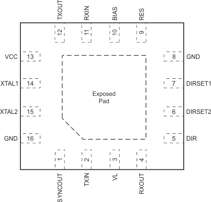
 Figure 5-1 RGT Package, 16-Pin VQFN, Top
View
Figure 5-1 RGT Package, 16-Pin VQFN, Top
ViewTable 5-1 Pin Functions
| PIN | DESCRIPTION | ||
|---|---|---|---|
| NAME | NO. | TYPE | |
| BIAS | 10 | O | Bias voltage output for setting driver output power by external resistors |
| DIR | 5 | O | Direction control output signal for bus arbitration |
| DIRSET1 | 7 | — | DIRSET1 and DIRSET2:
Bits to set the duration of DIR DIRSET[2:1]: [L:L] = 9.6 kbps; [L:H] = 38.4 kbps; [H:L] = 115 kbps; [H:H] = standby mode |
| DIRSET2 | 6 | — | |
| GND | 8 | — | Ground |
| 16 | |||
| RES | 9 | P | Input voltage to adjust driver output power that is set by external resistors from BIAS pin to GND |
| RXIN | 11 | I | Modulated input signal to the receiver |
| RXOUT | 4 | O | Digital data bit stream from receiver |
| SYNCOUT | 1 | O | Open-drain output to synchronize other devices to the 4x-carrier oscillator at XTAL1 and XTAL2 |
| TXIN | 2 | I | Digital data bit stream to driver |
| TXOUT | 12 | O | Modulated output signal from the driver |
| VCC | 13 | P | Analog supply voltage for the device |
| VL | 3 | P | Logic supply voltage for the device |
| XTAL1 | 14 | I/O | I/O pins of the crystal oscillator. Connect a 4 × fC crystal between these pins or connect XTAL1 to an 8.704-MHz clock and connect XTAL2 to GND. |
| XTAL2 | 15 | ||
| EP | — | — | Exposed pad. Connection to ground plane is recommended for best thermal conduction. |