SLLSE11H March 2012 – March 2019 SN65HVD72 , SN65HVD75 , SN65HVD78
UNLESS OTHERWISE NOTED, this document contains PRODUCTION DATA.
- 1 Features
- 2 Applications
- 3 Description
- 4 Revision History
- 5 Device Comparison Table
- 6 Pin Configuration and Functions
-
7 Specifications
- 7.1 Absolute Maximum Ratings
- 7.2 ESD Ratings
- 7.3 Recommended Operating Conditions
- 7.4 Thermal Information
- 7.5 Electrical Characteristics
- 7.6 Power Dissipation
- 7.7 Switching Characteristics: 250 kbps Device (SN65HVD72) Bit Time ≥ 4 µs
- 7.8 Switching Characteristics: 20 Mbps Device (SN65HVD75) Bit Time ≥50 ns
- 7.9 Switching Characteristics: 50 Mbps Device (SN65HVD78) Bit Time ≥20 ns
- 7.10 Typical Characteristics
- 8 Parameter Measurement Information
- 9 Detailed Description
- 10Application and Implementation
- 11Power Supply Recommendations
- 12Layout
- 13Device and Documentation Support
- 14Mechanical, Packaging, and Orderable Information
Package Options
Mechanical Data (Package|Pins)
Thermal pad, mechanical data (Package|Pins)
- DRB|8
Orderable Information
10.2.1.5 Transient Protection
The bus pins of the SN65HVD7x transceiver family possess on-chip ESD protection against ±15-kV human body model (HBM) and ±12-kV IEC 61000-4-2 contact discharge. The IEC-ESD test is far more severe than the HBM-ESD test. The 50% higher charge capacitance, CS, and 78% lower discharge resistance, RD, of the IEC-model produce significantly higher discharge currents than the HBM-model.
As stated in the IEC 61000-4-2 standard, contact discharge is the preferred test method; although IEC air-gap testing is less repeatable than contact testing, air discharge protection levels are inferred from the contact discharge test results.
 Figure 23. HBM and IEC-ESD Models and Currents in Comparison (HBM Values in Parenthesis)
 The on-chip implementation of IEC ESD protection significantly increases the robustness of equipment. Common discharge events occur due to human contact with connectors and cables. Designers may choose to implement protection against longer duration transients, typically referred to as surge transients.
EFTs are generally caused by relay-contact bounce or the interruption of inductive loads. Surge transients often result from lightning strikes (direct strike or an indirect strike which induce voltages and currents), or the switching of power systems, including load changes and short circuit switching. These transients are often encountered in industrial environments, such as factory automation and power-grid systems.
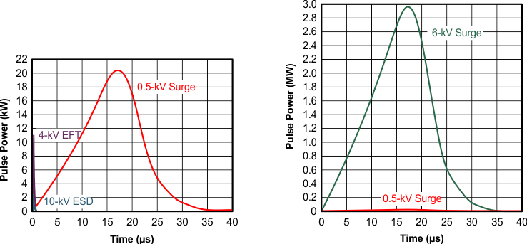
Figure 24 compares the pulse-power of the EFT and surge transients with the power caused by an IEC ESD transient. The left-hand diagram shows the relative pulse-power for a 0.5-kV surge transient and 4-kV EFT transient, both of which dwarf the 10-kV ESD transient visible in the lower-left corner. 500-V surge transients are representative of events that may occur in factory environments in industrial and process automation.
The right-hand diagram shows the pulse-power of a 6-kV surge transient, relative to the same 0.5-kV surge transient. 6-kV surge transients are most likely to occur in power generation and power-grid systems.
 Figure 24. Power Comparison of ESD, EFT, and Surge Transients
 In the case of surge transients, high-energy content is characterized by long pulse duration and slow decaying pulse power. The electrical energy of a transient that is dumped into the internal protection cells of a transceiver is converted into thermal energy which heats and destroys the protection cells, thus destroying the transceiver. Figure 25 shows the large differences in transient energies for single ESD, EFT, and surge transients, as well as for an EFT pulse train, commonly applied during compliance testing.
 Figure 25. Comparison of Transient Energies