SLLSE11H March   2012  – March 2019 SN65HVD72 , SN65HVD75 , SN65HVD78

UNLESS OTHERWISE NOTED, this document contains PRODUCTION DATA.  

  1. Features
  2. Applications
  3. Description
    1.     Device Images
      1.      Typical Application Diagram
  4. Revision History
  5. Device Comparison Table
  6. Pin Configuration and Functions
    1.     Pin Functions
  7. Specifications
    1. 7.1  Absolute Maximum Ratings
    2. 7.2  ESD Ratings
    3. 7.3  Recommended Operating Conditions
    4. 7.4  Thermal Information
    5. 7.5  Electrical Characteristics
    6. 7.6  Power Dissipation
    7. 7.7  Switching Characteristics: 250 kbps Device (SN65HVD72) Bit Time ≥ 4 µs
    8. 7.8  Switching Characteristics: 20 Mbps Device (SN65HVD75) Bit Time ≥50 ns
    9. 7.9  Switching Characteristics: 50 Mbps Device (SN65HVD78) Bit Time ≥20 ns
    10. 7.10 Typical Characteristics
  8. Parameter Measurement Information
  9. Detailed Description
    1. 9.1 Overview
    2. 9.2 Functional Block Diagram
    3. 9.3 Feature Description
    4. 9.4 Device Functional Modes
  10. 10Application and Implementation
    1. 10.1 Application Information
    2. 10.2 Typical Application
      1. 10.2.1 Design Requirements
        1. 10.2.1.1 Data Rate and Bus Length
        2. 10.2.1.2 Stub Length
        3. 10.2.1.3 Bus Loading
        4. 10.2.1.4 Receiver Failsafe
        5. 10.2.1.5 Transient Protection
      2. 10.2.2 Detailed Design Procedure
        1. 10.2.2.1 External Transient Protection
        2. 10.2.2.2 Isolated Bus Node Design
      3. 10.2.3 Application Curves
  11. 11Power Supply Recommendations
  12. 12Layout
    1. 12.1 Layout Guidelines
    2. 12.2 Layout Example
  13. 13Device and Documentation Support
    1. 13.1 Device Support
      1. 13.1.1 Third-Party Products Disclaimer
    2. 13.2 Documentation Support
      1. 13.2.1 Related Documentation
    3. 13.3 Related Links
    4. 13.4 Community Resources
    5. 13.5 Trademarks
    6. 13.6 Electrostatic Discharge Caution
    7. 13.7 Glossary
  14. 14Mechanical, Packaging, and Orderable Information

Package Options

Mechanical Data (Package|Pins)
Thermal pad, mechanical data (Package|Pins)
Orderable Information

Typical Characteristics

SN65HVD72 SN65HVD75 SN65HVD78 drvo_io_llsE11.gifFigure 1. Driver Output Voltage vs Driver Output Current
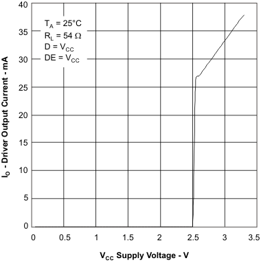
SN65HVD72 SN65HVD75 SN65HVD78 io_vcc_4_llsE11.gifFigure 3. Driver Output Current vs Supply Voltage
SN65HVD72 SN65HVD75 SN65HVD78 Driver_prop_delay_HVD78_llsE11.gifFigure 5. SN65HVD78 Driver Propagation Delay vs Temperature
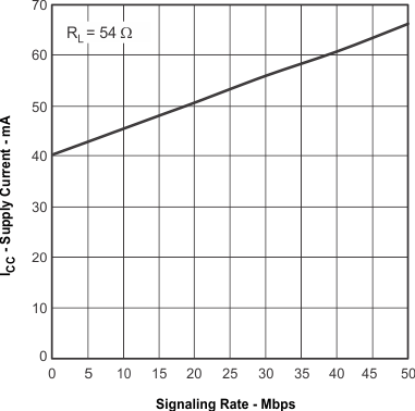
SN65HVD72 SN65HVD75 SN65HVD78 sup_cur_HVD75_llsE11.gifFigure 7. SN65HVD75 Supply Current vs Signal Rate
SN65HVD72 SN65HVD75 SN65HVD78 rec_outin_llsE11.gifFigure 9. Receiver Output vs Input
SN65HVD72 SN65HVD75 SN65HVD78 difvo_io_llsE11.gifFigure 2. Driver Differential Output Voltage vs Driver Output Current
SN65HVD72 SN65HVD75 SN65HVD78 Driver_rise_fall_HVD78_llsE11.gifFigure 4. SN65HVD78 Driver Rise or Fall Time vs Temperature
SN65HVD72 SN65HVD75 SN65HVD78 sup_cur_HVD72_llsE11.gifFigure 6. SN65HVD72 Supply Current vs Signal Rate
SN65HVD72 SN65HVD75 SN65HVD78 sup_cur_HVD78_llsE11.gifFigure 8. SN65HVD78 Supply Current vs Signal Rate