SLIS128D November 2011 – April 2022 SN65HVDA100-Q1
PRODUCTION DATA
- 1 Features
- 2 Applications
- 3 Description
- 4 Description (continued)
- 5 Revision History
- 6 Pin Configuration and Functions
- 7 Specifications
- 8 Parameter Measurement Information
-
9 Detailed Description
- 9.1 Overview
- 9.2 Functional Block Diagram
- 9.3
Feature Description
- 9.3.1 LIN (Local Interconnect Network) Bus
- 9.3.2 TXD (Transmit Input / Output)
- 9.3.3 RXD (Receive Output)
- 9.3.4 VSUP (Supply Voltage)
- 9.3.5 GND (Ground)
- 9.3.6 EN (Enable Input)
- 9.3.7 NWake (High Voltage Wake Up Input)
- 9.3.8 INH (Inhibit Output)
- 9.3.9 TXD Dominant State Timeout
- 9.3.10 Thermal Shutdown
- 9.3.11 Bus Stuck Dominant System Fault: False Wake-Up Lockout
- 9.3.12 Undervoltage on VSUP
- 9.3.13 Unpowered Device Does Not Affect the LIN Bus
- 9.4 Device Functional Modes
- 10Application and Implementation
- 11Power Supply Recommendations
- 12Layout
- 13Device and Documentation Support
- 14Mechanical, Packaging, and Orderable Information
Package Options
Mechanical Data (Package|Pins)
- D|8
Thermal pad, mechanical data (Package|Pins)
Orderable Information
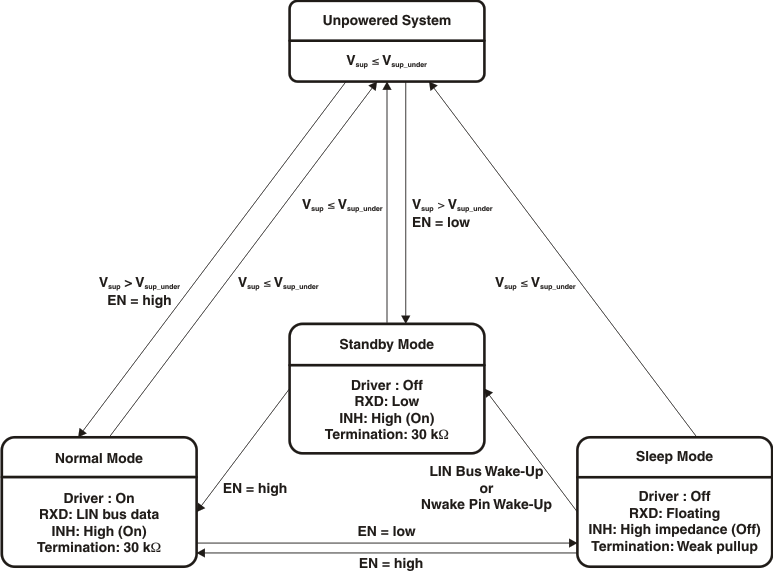
9.4.1 Operating States
 Figure 9-4 Operating States Diagram
Table 9-1 Operating Modes
| MODE | EN | RXD | LIN BUS TERMINATION | INH | TRANSMITTER | COMMENTS |
|---|---|---|---|---|---|---|
| Sleep | Low | Floating | Weak current pullup | High impedance | Off | |
| Standby | Low | Low | 30 kΩ (typical) | High | Off | Wake-up event detected, waiting on MCU to set EN |
| Normal | High | LIN bus data | 30 kΩ (typical) | High | On | LIN transmission up to 20 kbps |