SLIS128D November 2011 – April 2022 SN65HVDA100-Q1
PRODUCTION DATA
- 1 Features
- 2 Applications
- 3 Description
- 4 Description (continued)
- 5 Revision History
- 6 Pin Configuration and Functions
- 7 Specifications
- 8 Parameter Measurement Information
-
9 Detailed Description
- 9.1 Overview
- 9.2 Functional Block Diagram
- 9.3
Feature Description
- 9.3.1 LIN (Local Interconnect Network) Bus
- 9.3.2 TXD (Transmit Input / Output)
- 9.3.3 RXD (Receive Output)
- 9.3.4 VSUP (Supply Voltage)
- 9.3.5 GND (Ground)
- 9.3.6 EN (Enable Input)
- 9.3.7 NWake (High Voltage Wake Up Input)
- 9.3.8 INH (Inhibit Output)
- 9.3.9 TXD Dominant State Timeout
- 9.3.10 Thermal Shutdown
- 9.3.11 Bus Stuck Dominant System Fault: False Wake-Up Lockout
- 9.3.12 Undervoltage on VSUP
- 9.3.13 Unpowered Device Does Not Affect the LIN Bus
- 9.4 Device Functional Modes
- 10Application and Implementation
- 11Power Supply Recommendations
- 12Layout
- 13Device and Documentation Support
- 14Mechanical, Packaging, and Orderable Information
Package Options
Mechanical Data (Package|Pins)
- D|8
Thermal pad, mechanical data (Package|Pins)
Orderable Information
3 Description
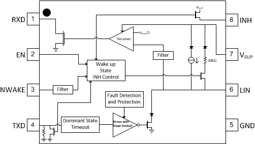
The SN65HVDA100-Q1 device is a Local Interconnect Network (LIN) physical interface, which integrates the serial transceiver with wakeup and protection features. The LIN bus is a single-wire bidirectional bus typically used for low-speed in-vehicle networks using data rates from 2.4 kbps to 20 kbps. The LIN protocol output data stream on TXD is converted by the SN65HVDA100-Q1 into the LIN bus signal through a current-limited wave-shaping driver as outlined by the LIN Physical Layer Specification and ISO 17987. The receiver converts the data stream from the LIN bus and outputs the data stream through RXD. The LIN bus has two states: dominant state (voltage near ground) and recessive state (voltage near battery). In the recessive state, the LIN bus is pulled high by the internal pullup resistor (30 kΩ) and series diode, so no external pullup components are required for responder applications. Commander applications require an external pullup resistor (1 kΩ) plus a series diode per the LIN specification.
| PART NUMBER | PACKAGE(1) | BODY SIZE (NOM) |
|---|---|---|
| SN65HVDA100-Q1 | SOIC (8) | 4.90 mm × 3.91 mm |
 SN65HVDA100-Q1 Block Diagram