-
SN65HVDA1040A-Q1 EMC-Optimized High-Speed CAN Bus Transceiver
- 1 Features
- 2 Applications
- 3 Description
- 4 Revision History
- 5 Pin Configuration and Functions
- 6 Specifications
- 7 Parameter Measurement Information
- 8 Detailed Description
- 9 Application and Implementation
- 10Power Supply Recommendations
- 11Layout
- 12Device and Documentation Support
- 13Mechanical, Packaging, and Orderable Information
- IMPORTANT NOTICE
Package Options
Mechanical Data (Package|Pins)
Thermal pad, mechanical data (Package|Pins)
- DSJ|12
Orderable Information
SN65HVDA1040A-Q1 EMC-Optimized High-Speed CAN Bus Transceiver
1 Features
- Qualified for Automotive Applications
- Meets or Exceeds the Requirements of ISO 11898-2 and -5
- GIFT/ICT Compliant
- ESD Protection up to ±12 kV (Human Body Model) on Bus Pins
- Low-Current Standby Mode With Bus Wakeup, <12 µA Maximum
- High Electromagnetic Compliance (EMC)
- SPLIT Voltage Source for Common-Mode Stabilization of Bus Through Split Termination
- Digital Inputs Compatible With 3.3-V and 5-V Microprocessors
- Package Options: SOIC and VSON
- Protection Features
- Bus-Fault Protection of –27 V to 40 V
- TXD Dominant Time-Out
- Thermal Shutdown Protection
- Power Up and Power Down Glitch-Free Bus Inputs and Outputs
- High Bus Input Impedance With Low VCC (Ideal Passive Behavior on Bus When Unpowered)
2 Applications
- GMW3122 Dual-Wire CAN Physical Layer
- SAE J2284 High-Speed CAN for Automotive Applications
- SAE J1939 Standard Data Bus Interface
- ISO 11783 Standard Data Bus Interface
- NMEA 2000 Standard Data Bus Interface
3 Description
The SN65HVDA1040A-Q1 device meets or exceeds the specifications of the ISO 11898 standard for use in applications employing a Controller Area Network (CAN). The device is qualified for use in automotive applications. As a CAN transceiver, this device provides differential transmit capability to the bus and differential receive capability to a CAN controller at signaling rates up to 1 megabit per second (Mbps). The signaling rate of a line is the number of voltage transitions that are made per second, expressed in the units bps (bits per second).
The device is designed for operation in especially harsh environments and includes many device protection features such as undervoltage lock out (UVLO), overtemperature thermal shutdown, wide common-mode range, and loss of ground protection. The bus pins are also protected against external cross-wiring, shorts to –27 V to 40 V, and voltage transients according to ISO 7637.
Device Information(1)
| PART NUMBER | PACKAGE | BODY SIZE (NOM) |
|---|---|---|
| SN65HVDA1040A-Q1 | VSON (12) | 3.00 mm × 4.00 mm |
| SOIC (8) | 4.90 mm × 3.91 mm |
- For all available packages, see the orderable addendum at the end of the data sheet.
Block Diagram

4 Revision History
Changes from C Revision (February 2011) to D Revision
- Added ESD Ratings table, Feature Description section, Device Functional Modes, Application and Implementation section, Power Supply Recommendations section, Layout section, Device and Documentation Support section, and Mechanical, Packaging, and Orderable Information section Go
5 Pin Configuration and Functions


Pin Functions
| PIN | TYPE | DESCRIPTION | ||
|---|---|---|---|---|
| NAME | SOIC | VSON | ||
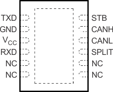
| TXD | 1 | 1 | I | CAN transmit data input (low for dominant bus state, high for recessive bus state) |
| GND | 2 | 2 | GND | Ground connection |
| VCC | 3 | 3 | Supply | Transceiver 5-V supply voltage input |
| RXD | 4 | 4 | O | CAN receive data output (low in domonint bus state, high in recessive bus state) |
| SPLIT | 5 | 9 | O | Common-mode stabilization output |
| CANL | 6 | 10 | I/O | Low-level CAN bus line |
| CANH | 7 | 11 | I/O | High-level CAN bus line |
| STB | 8 | 12 | I | Standby mode select pin (active high) |
| NC | — | 5-8 | NC | No connect |
6 Specifications
6.1 Absolute Maximum Ratings
over operating free-air temperature range (unless otherwise noted) (1)| MIN | MAX | UNIT | ||
|---|---|---|---|---|
| VCC | Supply voltage | –0.3 | 6 | V |
| Voltage range at bus terminals (CANH, CANL, SPLIT) | –27 | 40 | V | |
| IO | Receiver output current | 20 | mA | |
| VI | Voltage input, ISO 7637 transient pulse(2) (CANH, CANL) | –150 | 100 | V |
| VI | Voltage input (TXD, STB) | –0.3 | 6 | V |
| TJ | Junction temperature | –40 | 150 | °C |
| Tstg | Storage temperature | –40 | 150 | °C |
6.2 ESD Ratings
| VALUE | UNIT | ||||
|---|---|---|---|---|---|
| V(ESD) | Electrostatic discharge | Human body model (HBM), per AEC Q100-002(1) | Pins 7 and 6(2) | ±12000 | V |
| Pin 5(3) | ±10000 | ||||
| All pins | ±4000 | ||||
| Charged-device model (CDM), per AEC Q100-011 | ±1500 | ||||
| Machine Model(4) | ±200 | ||||
| IEC 61000-4-2 according to IBEE CAN EMC test specification | Pins 7 and 6 connected to pin 2 | ±7000 | |||
6.3 Recommended Operating Conditions
| MIN | MAX | UNIT | |||
|---|---|---|---|---|---|
| VCC | Supply voltage | 4.75 | 5.25 | V | |
| VI or VIC | Voltage at any bus terminal (separately or common mode) | –12 | 12 | V | |
| VIH | High-level input voltage | TXD, STB | 2 | 5.25 | V |
| VIL | Low-level input voltage | TXD, STB | 0 | 0.8 | V |
| VID | Differential input voltage | –6 | 6 | V | |
| IOH | High-level output current | Driver | –70 | mA | |
| Receiver (RXD) | –2 | ||||
| IOL | Low-level output current | Driver | 70 | mA | |
| Receiver (RXD) | 2 | ||||
| TA | Operating free-air temperature range | See Thermal Information | –40 | 125 | °C |
6.4 Thermal Information
| THERMAL METRIC(1) | SN65HVDA1040A-Q1 | UNIT | |||
|---|---|---|---|---|---|
| DSG (VSON) | D (SOIC) |
||||
| 12 PINS | 8 PINS | ||||
| RθJA | Junction-to-ambient thermal resistance | Low-K thermal resistance(2) | 290 | 140 | °C/W |
| High-K thermal resistance(3) | 52 | 112 | °C/W | ||
| RθJC(top) | Junction-to-case (top) thermal resistance | 56 | 56 | °C/W | |
| RθJB | Junction-to-board thermal resistance | 14 | 50 | °C/W | |
| ψJT | Junction-to-top characterization parameter | 6 | 13 | °C/W | |
| ψJB | Junction-to-board characterization parameter | 19 | 55 | °C/W | |
| RθJC(bot) | Junction-to-case (bottom) thermal resistance | 4.5 | – | °C/W | |
6.5 Electrical Characteristics
over recommended operating conditions including operating free-air temperature range (unless otherwise noted)| PARAMETER | TEST CONDITIONS | MIN | TYP(1) | MAX | UNIT | ||
|---|---|---|---|---|---|---|---|
| SUPPLY | |||||||
| ICC | 5-V supply current | Standby mode | STB at VCC, VI = VCC | 6 | 12 | µA | |
| Dominant | VI = 0 V, 60-Ω load, STB at 0 V | 50 | 70 | mA | |||
| Recessive | VI = VCC, No load, STB at 0 V | 6 | 10 | ||||
| UVVCC | Undervoltage reset threshold | 2.8 | 4 | V | |||
| DRIVER | |||||||
| VO(D) | Bus output voltage (dominant) | CANH | VI = 0 V, STB at 0 V, RL = 60 Ω, See Figure 3 and Figure 16 |
2.9 | 3.4 | 4.5 | V |
| CANL | 0.8 | 1.75 | |||||
| VO(R) | Bus output voltage (recessive) | VI = 3 V, STB at 0 V, RL = 60 Ω, See Figure 3 and Figure 16 |
2 | 2.5 | 3 | V | |
| VO | Bus output voltage (standby mode) | STB at Vcc, RL = 60 Ω, See Figure 3 and Figure 16 |
–0.1 | 0.1 | V | ||
| VOD(D) | Differential output voltage (dominant) | VI = 0 V, RL = 60 Ω, STB at 0 V, See Figure 3, Figure 16, and Figure 4 |
1.5 | 3 | V | ||
| VI = 0 V, RL = 45 Ω, STB at 0 V, See Figure 3, Figure 16, and Figure 4 |
1.4 | 3 | |||||
| VOD(R) | Differential output voltage (recessive) | VI = 3 V, STB at 0 V, RL = 60 Ω, See Figure 3 and Figure 16 |
–0.012 | 0.012 | V | ||
| VI = 3 V, STB at 0 V, No load | –0.5 | 0.05 | |||||
| VSYM | Output symmetry (dominant or recessive) (VO(CANH) + VO(CANL)) | STB at 0 V, RL = 60 Ω, See Figure 14 | 0.9 VCC | VCC | 1.1 VCC | V | |
| VOC(ss) | Steady-state common-mode output voltage | STB at 0 V, RL = 60 Ω, See Figure 9 | 2 | 2.5 | 3 | V | |
| ΔVOC(ss) | Change in steady-state common-mode output voltage | STB at 0 V, RL = 60 Ω, See Figure 9 | 30 | mV | |||
| VIH | High-level input voltage, TXD input | 2 | V | ||||
| VIL | Low-level input voltage, TXD input | 0.8 | V | ||||
| IIH | High-level input current, TXD input | VI at VCC | –2 | 2 | µA | ||
| IIL | Low-level input current, TXD input | VI at 0 V | –50 | –10 | µA | ||
| IO(off) | Power-off TXD output current | VCC at 0 V, TXD at 5 V | 1 | µA | |||
| IOS(ss) | Short-circuit steady-state output current, Dominant | VCANH = –12 V, CANL open, TXD = low, See Figure 12 |
–120 | –85 | mA | ||
| VCANH = 12 V, CANL open, TXD = low, See Figure 12 |
0.4 | 1 | |||||
| VCANL = –12 V, CANH open, TXD = low, See Figure 12 |
–1 | –0.6 | |||||
| VCANL = 12 V, CANH open, TXD = low, See Figure 12 |
75 | 120 | |||||
| VCANH = 0 V, CANL open, TXD = low, See Figure 12 |
–100 | –75 | |||||
| VCANL = 32 V, CANH open, , TXD = low, See Figure 12 |
75 | 125 | |||||
| IOS(ss) | Short-circuit steady-state output current, Recessive | –20 V ≤ VCANH ≤ 32 V, CANL open, TXD = high, See Figure 12 |
–10 | 10 | mA | ||
| –20 V ≤ VCANL ≤ 32 V, CANH open, TXD = high, See Figure 12 |
–10 | 10 | |||||
| CO | Output capacitance | See receiver input capacitance | |||||
| RECEIVER | |||||||
| VIT+ | Positive-going input threshold voltage, high-speed mode | STB at 0 V, See Table 1 | 800 | 900 | mV | ||
| VIT– | Negative-going input threshold voltage, high-speed mode | STB at 0 V, See Table 1 | 500 | 650 | mV | ||
| Vhys | Hysteresis voltage (VIT+ – VIT–) | 100 | 125 | mV | |||
| VIT | Input threshold voltage, standby mode | STB at VCC | 500 | 1150 | mV | ||
| VOH | High-level output voltage | IO = –2 mA, See Figure 7 | 4 | 4.6 | V | ||
| VOL | Low-level output voltage | IO = 2 mA, See Figure 7 | 0.2 | 0.4 | V | ||
| II(off) | Power-off bus input current (unpowered bus leakage current) | CANH = CANL = 5 V, VCC at 0 V, TXD at 0 V |
3 | µA | |||
| IO(off) | Power-off RXD leakage current | VCC at 0 V, RXD at 5 V | 20 | µA | |||
| CI | Input capacitance to ground (CANH or CANL) | TXD at 3 V, VI = 0.4 sin (4E6πt) + 2.5 V |
13 | pF | |||
| CID | Differential input capacitance | TXD at 3 V, VI = 0.4 sin (4E6πt) | 6 | pF | |||
| RID | Differential input resistance | TXD at 3 V, STB at 0 V | 30 | 80 | kΩ | ||
| RIN | Input resistance (CANH or CANL) | TXD at 3 V, STB at 0 V | 15 | 30 | 40 | kΩ | |
| RI(m) | Input resistance matching [1 – (RIN (CANH) / RIN (CANL))] × 100% |
V(CANH) = V(CANL) | –3% | 0% | 3% | ||
| STB PIN | |||||||
| VIH | High-level input voltage, STB input | 2 | V | ||||
| VIL | Low-level input voltage, STB input | 0.8 | V | ||||
| IIH | High-level input current | STB at 2 V | –10 | 0 | µA | ||
| IIL | Low-level input current | STB at 0.8 V | –10 | 0 | µA | ||
| SPLIT PIN | |||||||
| VO | Output voltage | –500 µA < IO < 500 µA | 0.3 VCC | 0.5 VCC | 0.7 VCC | V | |
| IO(stb) | Leakage current, standby mode | STB at 2 V, –12 V ≤ VO ≤ 12 V | –5 | 5 | µA | ||
6.6 Power Dissipation Characteristics
over recommended operating conditions, TA = –40°C to 125°C (unless otherwise noted)| TEST CONDITIONS | MIN | TYP | MAX | UNIT | ||
|---|---|---|---|---|---|---|
| PD | Average power dissipation | VCC = 5 V, TJ = 27°C, RL = 60 Ω, STB at 0 V, Input to TXD at 500 kHz, 50% duty cycle square wave, CL at RXD = 15 pF |
112 | mW | ||
| VCC = 5.5 V, TJ = 130°C, RL = 45 Ω, STB at 0 V, Input to TXD at 500 kHz, 50% duty cycle square wave, CL at RXD = 15 pF |
170 | |||||
| Thermal shutdown temperature | 185 | °C | ||||
6.7 Switching Characteristics
over operating free-air temperature range (unless otherwise noted)| PARAMETER | TEST CONDITIONS | MIN | TYP | MAX | UNIT | |
|---|---|---|---|---|---|---|
| DEVICE SWITCHING CHARACTERISTICS | ||||||
| td(LOOP1) | Total loop delay, driver input to receiver output, recessive to dominant | STB at 0 V, See Figure 10 | 90 | 230 | ns | |
| td(LOOP2) | Total loop delay, driver input to receiver output, dominant to recessive | STB at 0 V, See Figure 10 | 90 | 230 | ns | |
| DRIVER SWITCHING CHARACTERISTICS | ||||||
| tPLH | Propagation delay time, low-to-high level output | STB at 0 V, See Figure 5 | 25 | 65 | 120 | ns |
| tPHL | Propagation delay time, high-to-low level output | STB at 0 V, See Figure 5 | 25 | 45 | 120 | ns |
| tr | Differential output signal rise time | STB at 0 V, See Figure 5 | 25 | ns | ||
| tf | Differential output signal fall time | STB at 0 V, See Figure 5 | 45 | ns | ||
| ten | Enable time from standby mode to normal mode and transmission of dominant | See Figure 8 | 10 | µs | ||
| t(dom) | Dominant time-out(1) | ↓VI, See Figure 11 | 300 | 450 | 700 | µs |
| RECEIVER SWITCHING CHARACTERISTICS | ||||||
| tPLH | Propagation delay time, low-to-high-level output | STB at 0 V , See Figure 7 | 60 | 90 | 130 | ns |
| tPHL | Propagation delay time, high-to-low-level output | STB at 0 V , See Figure 7 | 45 | 70 | 130 | ns |
| tr | Output signal rise time | STB at 0 V , See Figure 7 | 8 | ns | ||
| tf | Output signal fall time | STB at 0 V , See Figure 7 | 8 | ns | ||
| tBUS | Dominant time required on bus for wakeup from standby | STB at VCC, See Figure 13 | 1.5 | 5 | µs | |
Minimum Bit Rate = 11/ t(dom) = 11 bits / 300 µs = 37 kbps
6.8 Typical Characteristics

vs Free-Air Temperature

vs. Supply Voltage
7 Parameter Measurement Information
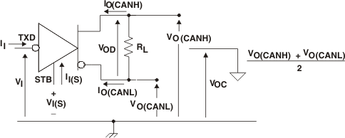
 Figure 3. Driver Voltage, Current, and Test Definition
 Figure 4. Driver VOD Test Circuit
 Figure 5. Driver Test Circuit and Voltage Waveforms
 Figure 6. Receiver Voltage and Current Definitions

Table 1. Differential Input Voltage Threshold Test
| INPUT | OUTPUT R |
|||
|---|---|---|---|---|
| VCANH | VCANL | |VID| | ||
| –11.1 V | –12 V | 900 mV | L | VOL |
| 12 V | 11.1 V | 900 mV | L | |
| –6 V | –12 V | 6 V | L | |
| 12 V | 6 V | 6 V | L | |
| –11.5 V | –12 V | 500 mV | H | VOH |
| 12 V | 11.5 V | 500 mV | H | |
| –12 V | –6 V | 6 V | H | |
| 6 V | 12 V | 6 V | H | |
| Open | Open | X | H | |


NOTE:
All VI input pulses are from 0 V to VCC and supplied by a generator having the following characteristics: tr or tf ≤ 6 ns, pulse repetition rate (PRR) = 125 kHz, 50% duty cycle.

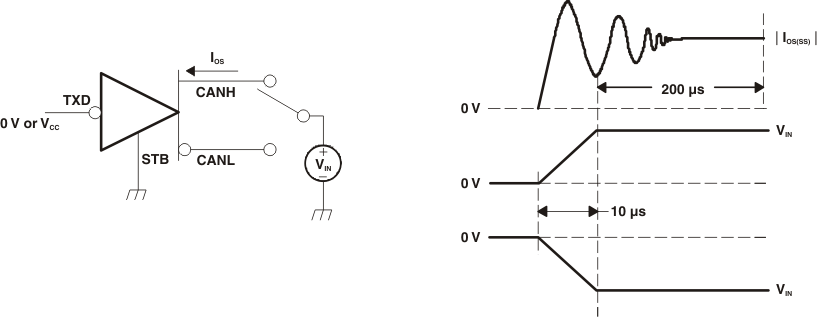
 Figure 12. Driver Short-Circuit Current Test and Waveforms


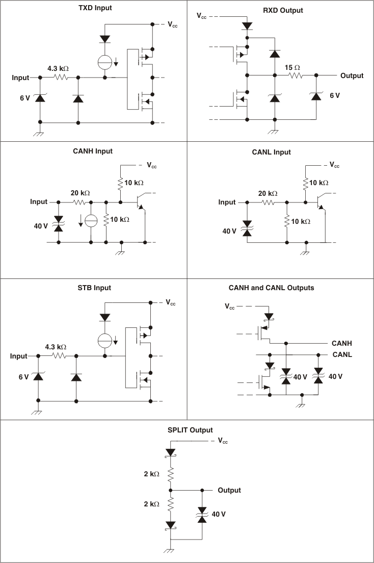
 Figure 15. Equivalent Input and Output Schematic Diagrams