SLASEE6 September 2016 SN65HVS883
PRODUCTION DATA.
- 1 Features
- 2 Applications
- 3 Description
- 4 Revision History
- 5 Pin Configuration and Functions
- 6 Specifications
- 7 Parameter Measurement Information
- 8 Detailed Description
- 9 Application and Implementation
- 10Power Supply Recommendations
- 11Layout
- 12Device and Documentation Support
- 13Mechanical, Packaging, and Orderable Information
Package Options
Mechanical Data (Package|Pins)
- PWP|28
Thermal pad, mechanical data (Package|Pins)
- PWP|28
Orderable Information
1 Features
- Eight Sensor Inputs
- High Input Voltage up to 34 V
- Selectable Debounce Filters
From 0 ms to 3 ms - Adjustable Current Limits
From 0.2 mA to 5.2 mA - Field Inputs and Supply Lines Protected
to 15-kV HBM
- Output Drivers for External Status LEDs
- Cascadable for More Inputs in Multiples of Eight
- SPI-Compatible Interface
- Regulated 5-V Output for External Digital Isolator
- Low-Supply Voltage Indicator
2 Applications
- Sensor Inputs for Industrial Automation and Process Control
- IEC61131-2 Type 1, 2, or 3 Switches
- EN60947-5-2 Proximity Switches
- High Channel Count Digital Input Modules for PC and PLC Systems
- Decentralized I/O Modules
3 Description
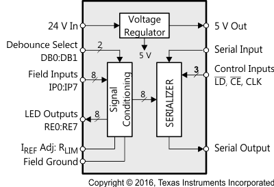
The SN65HVS883 is a 24-V, eight-channel, digital-input serializer for high-channel density digital input modules of PC and PLC-based systems in industrial automation. In combination with galvanic isolators, the device completes the interface between the 24-V sensor outputs of the field-side and the low-voltage controller inputs at the control-side. Input signals provided by EN60947-5-2 compliant 2-wire and
3-wire proximity switches are current-limited and then validated by internal debounce filters. The input switching characteristic is in accordance with IEC61131-2 for Type 1, 2, and 3 sensor switches.
Upon the application of load and clock signals, input data is latched in parallel into the shift register and afterwards clocked out serially via a subsequent isolator into a serial PLC input.
Cascading of multiple SN65HVS883 is possible by connecting the serial output of the leading device with the serial input of the following device, enabling the design of high-channel count input modules. Input status is indicated via 3-mA constant current LED outputs. An external precision resistor is required to set the internal reference current. The integrated voltage regulator provides a 5-V output to supply low-power isolators. An internal supply voltage monitor provides a chip-okay (CHOK) indication.
The SN65HVS883 comes in a 28-pin PWP PowerPAD™ package allowing for efficient heat dissipation. The device is specified for operation at temperatures from –40°C to 85°C.
Device Information(1)
| PART NUMBER | PACKAGE | BODY SIZE (NOM) |
|---|---|---|
| SN65HVS883 | HTSSOP (28) | 9.70 mm x 4.40 mm |
- For all available packages, see the orderable addendum at the end of the data sheet.
Simplified I/O Structure
